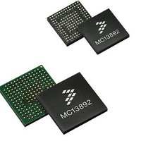
MC13892BJVL Freescale Semiconductor, MC13892BJVL Datasheet - Page 67

MC13892BJVL
Manufacturer Part Number
MC13892BJVL
Description
IC PMU I.MX51/37/35/27 186MAPBGA
Manufacturer
Freescale Semiconductor
Datasheets
1.MC13892AJVLR2.pdf
(156 pages)
2.MC13892AJVLR2.pdf
(2 pages)
3.MC13892AJVLR2.pdf
(16 pages)
4.MC13892AJVLR2.pdf
(5 pages)
Specifications of MC13892BJVL
Applications
Battery Management, Display (LED Drivers), Handheld/Mobile Devices, Power Supply
Operating Temperature
-40°C ~ 85°C
Mounting Type
Surface Mount
Package / Case
186-LFBGA
Mounting Style
SMD/SMT
Duty Cycle (max)
55 %
Input Voltage
- 0.3 V to + 20 V
Maximum Operating Temperature
+ 85 C
Minimum Operating Temperature
- 30 C
Output Current
30 mA
Output Voltage
3.3 V
Topology
Boost
Lead Free Status / RoHS Status
Lead free / RoHS Compliant
Current - Supply
-
Voltage - Supply
-
Lead Free Status / Rohs Status
Lead free / RoHS Compliant
Available stocks
Company
Part Number
Manufacturer
Quantity
Price
Company:
Part Number:
MC13892BJVL
Manufacturer:
Freescale Semiconductor
Quantity:
10 000
Company:
Part Number:
MC13892BJVLR2
Manufacturer:
Freescale Semiconductor
Quantity:
10 000
handled in a controlled slope manner, see Supplies, for details. Each switcher has an associated set of SPI bits for Standby mode
set points. By default the Standby settings are identical to the non-Standby settings, which are initially defined by PUMS
programming.
back what is programmed in SWxMODE[3:0], not the actual state that may be altered as described previously.
should use the Standby set point as programmed by SWxSTBY[4:0]. The activated switcher(s) will maintain settings for mode
and voltage until the next startup event. When the respective time slot of the startup sequencer is reached for a given switcher,
its mode and voltage settings will be updated the same as if starting out of the Off state (except that switchers active through a
Low Power Off mode will not be off when the startup sequencer is started).
POWER GATING SYSTEM
keeps the external memory powered for self refresh, and User Off, which keeps the processor powered up for state retention.
For reduced current drain in Low Power Off states, parts of the system can benefit from power gating to isolate the minimum
essentials for such operational modes. It is also necessary to ensure that the power budget on backed up domains are within the
capabilities of switchers in PFM mode. An additional benefit of power gating peripheral loads during system startup is to enable
the processor core to complete booting, and begin running software before additional supplies or peripheral devices are powered.
This allows system software to bring up the additional supplies and close power gating switches in the most optimum order, to
avoid problems with supply sequencing or transient current surges. The power gating switch drivers and integrated control are
included for optimizing the system power tree.
of PWGT1 for core supply power gating and PWGT2 for Memory Hold power gating.
USER OFF POWER GATING
PWGTDRV1 is provided for power gating peripheral loads sharing the processor core supply domain(s) SW1, and/or SW2, and/
or SW3. In addition, PWGTDRV2 is provided support to power gate peripheral loads on the SW4 supply domain.
Analog Integrated Circuit Device Data
Freescale Semiconductor
In addition to controlling the operating mode in Standby, the voltage setting can be changed. The transition in voltage is
The actual operating mode of the switchers as a function of STANDBY pins is not reflected through the SPI. The SPI will read
Table 35
The Low Power Off states are provided to allow faster system booting from two pseudo Off conditions: Memory Hold, which
The power gate drivers could be used for other general power gating as well. The text herein assumes the standard application
User Off configuration maintains PFM mode switchers on both the processor and external memory power domains.
and
Table 36
Table 36. Switcher Control In User Off
Notes
Table 35. Switcher Control In Memory Hold
Notes
53.
Table 34. Switcher Mode Control for Normal and Standby Operation
52.
Notes
51.
For User Off mode, an activated SWx should use the Standby set point as programmed by
SWxSTBY[4:0].
show the switcher mode control in the Low Power Off states. Note that a Low Power Off activated SWx
SWxMODE[3:0]
For Memory Hold mode, an activated SWx should use the Standby set point as programmed
by SWxSTBY[4:0].
STANDBY defined as logical AND of STANDBY and STANDBYSEC pin
SWxMHMODE
SWxUOMODE
1110
1111
0
1
0
1
Normal mode
PWMPS
PFM
Memory Hold Operational Mode
(51)
User Off Operational Mode
PFM
Off
PFM
Off
Standby Mode
PFM
PFM
(53)
FUNCTIONAL DEVICE OPERATION
(52)
(51)
OPERATING MODES
13892
67


