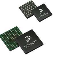
MC13892BJVL Freescale Semiconductor, MC13892BJVL Datasheet - Page 35

MC13892BJVL
Manufacturer Part Number
MC13892BJVL
Description
IC PMU I.MX51/37/35/27 186MAPBGA
Manufacturer
Freescale Semiconductor
Datasheets
1.MC13892AJVLR2.pdf
(156 pages)
2.MC13892AJVLR2.pdf
(2 pages)
3.MC13892AJVLR2.pdf
(16 pages)
4.MC13892AJVLR2.pdf
(5 pages)
Specifications of MC13892BJVL
Applications
Battery Management, Display (LED Drivers), Handheld/Mobile Devices, Power Supply
Operating Temperature
-40°C ~ 85°C
Mounting Type
Surface Mount
Package / Case
186-LFBGA
Mounting Style
SMD/SMT
Duty Cycle (max)
55 %
Input Voltage
- 0.3 V to + 20 V
Maximum Operating Temperature
+ 85 C
Minimum Operating Temperature
- 30 C
Output Current
30 mA
Output Voltage
3.3 V
Topology
Boost
Lead Free Status / RoHS Status
Lead free / RoHS Compliant
Current - Supply
-
Voltage - Supply
-
Lead Free Status / Rohs Status
Lead free / RoHS Compliant
Available stocks
Company
Part Number
Manufacturer
Quantity
Price
Company:
Part Number:
MC13892BJVL
Manufacturer:
Freescale Semiconductor
Quantity:
10 000
Company:
Part Number:
MC13892BJVLR2
Manufacturer:
Freescale Semiconductor
Quantity:
10 000
REGULATORS
VINIOHI
VIOHI
VINPLL AND VINDIG
either BP or a 1.8 V switched mode power supply rail, such as from SW4 for the two lower set points of each regulator (the 1.2
and 1.25 V output for VPLL, and 1.05 and 1.25 V output for VDIG). In addition, when the two upper set points are used (1.50 and
1.8V outputs for VPLL, and 1.65 and 1.8V for VDIG), they can be connected to either BP or a 2.2V nominal external switched
mode power supply rail, to improve power dissipation.
VPLL
VDIG
VVIDEODRV
VVIDEO
VINAUDIO
VAUDIO
VINUSB2
VUSB2
VINCAMDRV
of the PNP in order to drive it.
VCAM
VSDDRV
VSD
Analog Integrated Circuit Device Data
Freescale Semiconductor
Input of VIOHI regulator. Connect this pin to BP in order to supply VIOHI regulator.
Output regulator for high voltage IO. Fixed 2.775 V output for high voltage level interface.
The input of the regulator for processor PLL and Digital regulators respectively. VINDIG and VINPLL can be connected to
Output of regulator for processor PLL. Quiet analog supply (PLL, GPS).
Output regulator Digital. Low voltage digital (DPLL, GPS).
Drive output for VVIDEO external PNP transistor.
Output regulator TV DAC. This pin must be connected to the collector of the external PNP transistor of the VVIDEO regulator.
Input regulator VAUDIO. Typically connected to BP.
Output regulator for audio supply.
Input regulator VUSB2. This pin must always be connected to BP even if the regulators are not used by the application.
Output regulator for powering USB PHY.
1. Input regulator camera using internal PMOS FET. Typically connected to BP.
2. Drive output regulator for camera voltage using external PNP device. In this case, this pin must be connected to the base
Output regulator for the camera module. When using an external PNP device, this pin must be connected to its collector.
Drive output for the VSD external PNP transistor.
Output regulator for multi-media cards such as micro SD, RS-MMC.
FUNCTIONAL PIN DESCRIPTION
FUNCTIONAL DESCRIPTION
13892
35


