FDD10N20LZTM Fairchild Semiconductor, FDD10N20LZTM Datasheet

MOSFET N-CH 200V 7.6A DPAK-3

FDD10N20LZTM

Manufacturer Part Number
FDD10N20LZTM
Description
MOSFET N-CH 200V 7.6A DPAK-3
Manufacturer
Fairchild Semiconductor
Series
UniFET™r
Datasheet

Specifications of FDD10N20LZTM

Input Capacitance (ciss) @ Vds
585pF @ 25V
Fet Type
MOSFET N-Channel, Metal Oxide
Fet Feature
Logic Level Gate
Rds On (max) @ Id, Vgs
360 mOhm @ 3.8A, 10V
Drain To Source Voltage (vdss)
200V
Current - Continuous Drain (id) @ 25° C
7.6A
Vgs(th) (max) @ Id
2.5V @ 250µA
Gate Charge (qg) @ Vgs
16nC @ 10V
Power - Max
56W
Mounting Type
Surface Mount
Package / Case
TO-252-3, DPak (2 Leads + Tab), SC-63
Transistor Polarity
N-Channel
Resistance Drain-source Rds (on)
0.3 Ohms
Forward Transconductance Gfs (max / Min)
8 S
Drain-source Breakdown Voltage
200 V
Continuous Drain Current
7.6 A
Power Dissipation
56 W
Maximum Operating Temperature
+ 150 C
Mounting Style
SMD/SMT
Lead Free Status / RoHS Status
Lead free / RoHS Compliant
©2010 Fairchild Semiconductor Corporation
FDD10N20LZ Rev. A
MOSFET Maximum Ratings
Thermal Characteristics
V
V
I
I
E
I
E
dv/dt
P
T
T
R
R
FDD10N20LZ
N-Channel MOSFET
200V Logic, 7.6A, 0.36
Features
• R
• Low Gate Charge ( Typ.12nC)
• Low C
• Fast Switching
• 100% Avalanche Tested
• Improved dv/dt Capability
• RoHS Compliant
D
DM
AR
J
L
DSS
GSS
AS
AR
D
JC
JA
, T
Symbol
Symbol
DS(on)
STG
rss
= 0.30( Typ.) @ V
( Typ.11pF)
Drain to Source Voltage
Gate to Source Voltage
Drain Current
Drain Current
Single Pulsed Avalanche Energy
Avalanche Current
Repetitive Avalanche Energy
Peak Diode Recovery dv/dt
Power Dissipation
Operating and Storage Temperature Range
Maximum Lead Temperature for Soldering Purpose,
1/8” from Case for 5 Seconds
Thermal Resistance, Junction to Case
Thermal Resistance, Junction to Ambient
GS
G
= 10V, I
S
D
= 3.8A
T
C
D-PAK
FDD- Series
= 25
Parameter
Parameter
-Continuous (T
-Continuous (T
- Pulsed
(T
- Derate above 25
C
o
= 25
C unless otherwise noted*
D
o
C)
C
C
= 25
= 100
o
1
C
o
Description
These N-Channel enhancement mode power field effect transistors
are produced using Fairchild’s proprietary, planar stripe, DMOS
technology.
This advance technology has been especially tailored to minimize
on-state resistance, provide superior switching performance, and
withstand high energy pulse in the avalanche and commutation
mode. These devices are well suited for high efficient switching
mode power supplies and active power factor correction.
C)
o
C)
(Note 1)
(Note 2)
(Note 1)
(Note 1)
(Note 3)
G
G
Typ
-
-
FDD10N20LZ
-55 to +150
D
D
S
S
0.45
200
±20
121
300
7.6
4.5
7.6
8.3
30
10
56
December 2010
UniFET
Max
110
2.2
www.fairchildsemi.com
Units
o
Units
C/W
W/
V/ns
mJ
mJ
o
o
W
V
V
A
A
A
C
C
o
C
TM

Related parts for FDD10N20LZTM

FDD10N20LZTM Summary of contents

Page 1

... Thermal Characteristics Symbol R Thermal Resistance, Junction to Case JC R Thermal Resistance, Junction to Ambient JA ©2010 Fairchild Semiconductor Corporation FDD10N20LZ Rev. A Description = 3.8A These N-Channel enhancement mode power field effect transistors D are produced using Fairchild’s proprietary, planar stripe, DMOS technology. This advance technology has been especially tailored to minimize ...

Page 2

Package Marking and Ordering Information Device Marking Device FDD10N20LZ FDD10N20LZ Electrical Characteristics Symbol Parameter Off Characteristics BV Drain to Source Breakdown Voltage DSS BV Breakdown Voltage Temperature DSS T Coefficient J I Zero Gate Voltage Drain Current DSS I Gate ...

Page 3

Typical Performance Characteristics Figure 1. On-Region Characteristics 10V 4.5V 4V 3.5V 1 0.1 0 Drain-Source Voltage[V] DS Figure 3. On-Resistance Variation vs. Drain Current and Gate Voltage 1.0 0.8 0.6 ...

Page 4

Typical Performance Characteristics Figure 7. Breakdown Voltage Variation vs. Temperature 1.2 1.1 1.0 0.9 0.8 -80 - Junction Temperature J Figure 9. Maximum Safe Operating Area - FDD10N20LZ 50 10 Operation in This Area 1 is ...

Page 5

FDD10N20LZ Rev. A Gate Charge Test Circuit & Waveform Resistive Switching Test Circuit & Waveforms Unclamped Inductive Switching Test Circuit & Waveforms 5 www.fairchildsemi.com ...

Page 6

Driver ) ( Driver ) DUT ) ( DUT ) DUT ) ( DUT ) FDD10N20LZ Rev. A Peak Diode Recovery dv/dt Test ...

Page 7

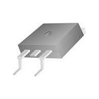
Mechanical Dimensions FDD10N20LZ Rev. A D-PAK 7 Dimensions in Millimeters www.fairchildsemi.com ...

Page 8

... TRADEMARKS The following includes registered and unregistered trademarks and service marks, owned by Fairchild Semiconductor and/or its global subsidiaries, and is not intended exhaustive list of all such trademarks. AccuPower™ Auto-SPM™ Build it Now™ CorePLUS™ CorePOWER™ CROSSVOLT ™ CTL™ ...

Related keywords