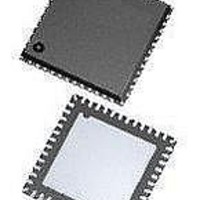
ASD5010L500INT Arctic Silicon Devices, ASD5010L500INT Datasheet - Page 31

ASD5010L500INT
Manufacturer Part Number
ASD5010L500INT
Description
ADC (A/D Converters) A-D Conv, Dig Gain Dual 8 bit 500MSPS
Manufacturer
Arctic Silicon Devices
Datasheet
1.ASD5010L500INT.pdf
(35 pages)
Specifications of ASD5010L500INT
Number Of Converters
2
Number Of Adc Inputs
4
Conversion Rate
500 MSPs
Resolution
8 bit
Snr
49.5 dB
Voltage Reference
1 V
Supply Voltage (max)
2 V
Supply Voltage (min)
1.7 V
Maximum Power Dissipation
295 mW
Maximum Operating Temperature
+ 85 C
Mounting Style
SMD/SMT
Package / Case
QFN-48
Input Voltage
1.8 V
Minimum Operating Temperature
- 40 C
Lead Free Status / RoHS Status
Lead free / RoHS Compliant
Preliminary Product Specification
Theory of Operation
ASD5010 is a multi Mode
consisting of 8 ADC branches, configured in different
channel modes, using interleaving to achieve high speed
sampling. For all practical purposes, the device can be
considered to contain 4 ADCs. Fine gain is adjusted for
each of the eight branches separately.
ASD5010 utilizes a LVDS output, described in 'Register
Description, LVDS Output Configuration and Control'. The
clocks needed (FCLK, LCLK) for the LVDS interface are
generated by an internal PLL.
The ASD5010 operate from one clock input, which can be
differential or single ended. The sampling clocks for each
of the four channels are generated from the clock input
using a carefully matched clock buffer tree. Internal clock
dividers are utilized to control the clock for each ADC
during interleaving. The clock tree is controlled by the
Mode of operations.
ASD5010 uses internally generated references. The
differential reference value is 1V. This results in a
differential input of −1V to correspond to the zero code of
the ADC, and a differential input of +1V to correspond to
the full-scale code (code 255).
The ADC employs a Pipeline converter architecture. Each
Pipeline Stage feeds its output data into the digital error
correction logic, ensuring excellent differential linearity
and no missing codes.
ASD5010 operates from two sets of supplies and
grounds. The analog supply and ground set is identified
as AVDD and AVSS, while the digital set is identified by
DVDD and DVSS.
Interleaving Effects and Sampling Order
Interleaving ADCs will generate interleaving artifacts
caused by gain, offset and timing mismatch between the
ADC branches. The design of ASD5010 has been
optimized to minimize these effects. It is not possible,
though, to eliminate mismatch completely, such that
additional compensation may be needed, especially when
using high digital gain settings. The internal digital fine
gain control may be used to compensate for gain errors
between the ADC branches. Due to the optimization of
ASD5010 there is not a one-to-one correspondence
between the sampling order, LVDS output order and the
branch number. Tables 23, 24 and 25 give an overview of
the corresponding branches, LVDS outputs and sampling
order for the different high speed modes.
ASD5010
Channel # Sampling order
1
2
3
4
Table 23: Quad channel mode
1
2
1
2
1
2
1
2
LVDS output
high-speed, CMOS ADC,
D1A
D1B
D2A
D2B
D3A
D3B
D4A
D4B
Fine gain
branch
1
2
3
4
5
6
7
8
rev 2.0, 2010.11.08
Page 31 of 35
Recommended Usage
Analog Input
The analog input to ASD5010 ADC is a switched
capacitor track-and-hold amplifier optimized for differential
operation.
Operation at common mode voltages at mid supply is
recommended even if performance will be good for the
ranges specified. The VCM pin provides a voltage
suitable as common mode voltage reference. The internal
buffer for the VCM voltage can be switched off, and
driving capabilities can be changed programming the
ext_vcm_bc<1:0> register.
Figure 12 shows a simplified drawing of the input
network. The signal source must have sufficiently low
output impedance to charge the sampling capacitors
within one clock cycle. A small external resistor (e.g. 22
ohm) in series with each input is recommended as it
helps reducing transient currents and dampens ringing
behavior. A small differential shunt capacitor at the chip
Channel # Sampling order
Channel # Sampling order
1
2
1
IPx
INx
Table 25: Single channel mode
Table 24: Dual channel mode
Figure 12: Input configuration
1
2
3
4
1
2
3
4
1
2
3
4
5
6
7
8
track
track
LVDS output
LVDS output
track
track
D1A
D1B
D2A
D2B
D3A
D3B
D4A
D4B
D1A
D1B
D2A
D2B
D3A
D3B
D4A
D4B
hold
hold
Fine gain
Fine gain
Confidential
branch
branch
1
3
2
4
5
7
6
8
1
6
2
5
8
3
7
4


