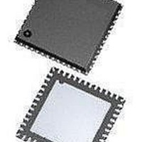
ASD5010L500INT Arctic Silicon Devices, ASD5010L500INT Datasheet - Page 15

ASD5010L500INT
Manufacturer Part Number
ASD5010L500INT
Description
ADC (A/D Converters) A-D Conv, Dig Gain Dual 8 bit 500MSPS
Manufacturer
Arctic Silicon Devices
Datasheet
1.ASD5010L500INT.pdf
(35 pages)
Specifications of ASD5010L500INT
Number Of Converters
2
Number Of Adc Inputs
4
Conversion Rate
500 MSPs
Resolution
8 bit
Snr
49.5 dB
Voltage Reference
1 V
Supply Voltage (max)
2 V
Supply Voltage (min)
1.7 V
Maximum Power Dissipation
295 mW
Maximum Operating Temperature
+ 85 C
Mounting Style
SMD/SMT
Package / Case
QFN-48
Input Voltage
1.8 V
Minimum Operating Temperature
- 40 C
Lead Free Status / RoHS Status
Lead free / RoHS Compliant
Preliminary Product Specification
Register Map
ASD5010
rst *
sleep4_ch<4:1>
sleep2_ch<2:1>
sleep1_ch1
sleep
pd
pd_pin_cfg<1:0>
ilvds_lclk<2:0>
ilvds_frame<2:0>
ilvds_dat<2:0>
en_lvds_term
term_lclk<2:0>
term_frame<2:0>
term_dat<2:0>
invert4_ch<4:1>
invert2_ch<2:1>
invert1_ch1
en_ramp
dual_custom_pat
single_custom_pat
bits_custom1
<7:0>
bits_custom2
<7:0>
cgain4_ch1 <3:0>
cgain4_ch2 <3:0>
cgain4_ch3 <3:0>
cgain4_ch4 <3:0>
cgain2_ch1 <3:0>
cgain2_ch2 <3:0>
Name
Self-clearing software reset.
Channel-specific sleep mode for a
Quad Channel setup.
Channel-specific sleep mode for a
Dual Channel setup.
Channel-specific sleep mode for a
Single Channel setup.
Go to sleep-mode.
Go to power-down.
Configures the PD pin function.
LVDS current drive programmability
for LCLKP and LCLKN pins.
LVDS current drive programmability
for FCLKP and FCLKN pins.
LVDS current drive programmability
for output data pins.
Enables internal termination for LVDS
buffers.
Programmable termination for LCLKN
and LCLKP buffers.
Programmable termination for FCLKN
and FCLKP buffers.
Programmable termination for output
data buffers.
Channel specific swapping of the
analog input signal for a Quad
Channel setup.
Channel specific swapping of the
analog input signal for a Dual
Channel setup.
Channel specific swapping of the
analog input signal for a Single
Channel setup.
Enables a repeating full-scale ramp
pattern on the outputs.
Enable the mode wherein the output
toggles between two defined codes.
Enables the mode wherein the output
is a constant specified code.
Bits for the single custom pattern and
for the first code of the dual custom
pattern.
Bits for the second code of the dual
custom pattern.
Programmable coarse gain channel 1
in a Quad Channel setup.
Programmable coarse gain channel 2
in a Quad Channel setup.
Programmable coarse gain channel 3
in a Quad Channel setup.
Programmable coarse gain channel 4
in a Quad Channel setup.
Programmable coarse gain channel 1
in a Dual Channel setup.
Programmable coarse gain channel 2
Description
Table 5: Register map – ASD5010
Termination disabled
Termination disabled
Termination disabled
Termination disabled
IPx is positive input
IPx is positive input
IPx is positive input
PD pin configured
for power-down
rev 2.0, 2010.11.08
3.5 mA drive
3.5 mA drive
3.5 mA drive
Default
Inactive
Inactive
Inactive
Inactive
Inactive
Inactive
Inactive
Inactive
Inactive
1x gain
1x gain
1x gain
1x gain
1x gain
1x gain
Page 15 of 35
mode
0x00
0x00
D15 D14D13D12D11D10 D9 D8 D7 D6 D5 D4 D3 D2 D1 D0
X
X
X
X
X
X
X
1
1
1
X
X
X
X
X
X
X
X
X
X
X
X X X
X X X
X X X
X X X
X X X
X
X
X X X X
X X X X
X
X X X
X X X
X
X 0 0
0 X 0
0 0 X
X X
X X
X X X X
X X X X
X X X X
X X X X
X X X
X X X
Confidential
X
Address
0x00
0x0F
0x12
0x24
0x25
0x26
0x27
0x2A
0x2B
Hex
0x11


