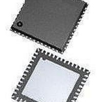
ASD5010L500INT Arctic Silicon Devices, ASD5010L500INT Datasheet - Page 25

ASD5010L500INT
Manufacturer Part Number
ASD5010L500INT
Description
ADC (A/D Converters) A-D Conv, Dig Gain Dual 8 bit 500MSPS
Manufacturer
Arctic Silicon Devices
Datasheet
1.ASD5010L500INT.pdf
(35 pages)
Specifications of ASD5010L500INT
Number Of Converters
2
Number Of Adc Inputs
4
Conversion Rate
500 MSPs
Resolution
8 bit
Snr
49.5 dB
Voltage Reference
1 V
Supply Voltage (max)
2 V
Supply Voltage (min)
1.7 V
Maximum Power Dissipation
295 mW
Maximum Operating Temperature
+ 85 C
Mounting Style
SMD/SMT
Package / Case
QFN-48
Input Voltage
1.8 V
Minimum Operating Temperature
- 40 C
Lead Free Status / RoHS Status
Lead free / RoHS Compliant
Preliminary Product Specification
The default data output format is offset binary. Two's complement mode can be selected by setting the btc_mode bit to '1'
which inverts the MSB.
The first bit of the frame (following the rising edge of FCLKP) is the LSB of the ADC output for default settings.
Programming the msb_first mode results in reverse bit order, and the MSB is output as the first bit following the FCLKP
rising edge.
LVDS Drive Strength Programmability
The current delivered by the LVDS output drivers can be configured as shown in table 18. The default current is 3.5mA,
which is what the LVDS standard specifies.
To reduce power consumption in the ASD5010, Reduced Swing Data Signaling (RSDS), is recommended. The output
current drive setting should then be 1.5 mA.
Setting the ilvds_lclk<2:0> register controls the current drive strength of the LVDS clock output on the LCLKP and
LCLKN pins.
Setting the ilvds_frame<2:0> register controls the current drive strength of the frame clock output on the FCLKP and
FCLKN pins.
Setting the ilvds_dat<2:0> register controls the current drive strength of the data outputs on the D[8:1]P and D[8:1]N
pins.
LVDS Internal Termination Programmability
The off-chip load on the LVDS buffers may represent a characteristic impedance that is not perfectly matched with the
ASD5010
ilvds_lclk<2:0>
ilvds_frame<2:0>
ilvds_dat<2:0>
en_lvds_term
term_lclk<2:0>
term_frame<2:0>
term_dat<2:0>
Name
Name
LVDS current drive programmability
for LCLKP and LCLKN pins.
LVDS current drive programmability
for FCLKP and FCLKN pins.
LVDS current drive programmability
for output data pins.
Enables internal termination for LVDS
buffers.
Programmable termination for LCLKN
and LCLKP buffers.
Programmable termination for FCLKN
and FCLKP buffers.
Programmable termination for output
data buffers.
Description
Description
Table 18: LVDS output drive strength for LCLK, FCLK and data
ilvds_*<2:0>
000
001
010
011
100
101
110
111
Termination disabled
Termination disabled
Termination disabled
Termination disabled
rev 2.0, 2010.11.08
3.5 mA drive
3.5 mA drive
3.5 mA drive
Default
Default
Page 25 of 35
LVDS drive strength
D15 D14D13D12D11D10 D9 D8 D7 D6 D5 D4 D3 D2 D1 D0
D15 D14D13D12D11D10 D9 D8 D7 D6 D5 D4 D3 D2 D1 D0
3.5 mA (default)
2.5 mA
1.5 mA (RSDS)
0.5 mA
7.5 mA
6.5 mA
5.5 mA
4.5 mA
X
1
1
1
X X X
X X X
X X X
X X X
X X X
X X X
Confidential
Address
Address
0x12
Hex
Hex
0x11


