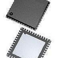
ASD5010L500INT Arctic Silicon Devices, ASD5010L500INT Datasheet - Page 24

ASD5010L500INT
Manufacturer Part Number
ASD5010L500INT
Description
ADC (A/D Converters) A-D Conv, Dig Gain Dual 8 bit 500MSPS
Manufacturer
Arctic Silicon Devices
Datasheet
1.ASD5010L500INT.pdf
(35 pages)
Specifications of ASD5010L500INT
Number Of Converters
2
Number Of Adc Inputs
4
Conversion Rate
500 MSPs
Resolution
8 bit
Snr
49.5 dB
Voltage Reference
1 V
Supply Voltage (max)
2 V
Supply Voltage (min)
1.7 V
Maximum Power Dissipation
295 mW
Maximum Operating Temperature
+ 85 C
Mounting Style
SMD/SMT
Package / Case
QFN-48
Input Voltage
1.8 V
Minimum Operating Temperature
- 40 C
Lead Free Status / RoHS Status
Lead free / RoHS Compliant
Preliminary Product Specification
To ease timing in the receiver when using multiple ASD5010, the device has the option to adjust the timing of the output
data and the frame clock. The propagation delay with respect to the ADC input clock can be moved one LVDS clock
cycle forward or backward, by using lvds_delay and lvds_advance, respectively. See figure 10 for details. Note that LCLK
is not affected by lvds_delay or lvds_advance settings.
The LVDS output interface of ASD5010 is a DDR interface. The default setting is with the LCLK rising and falling edge
transitions in the middle of alternate data windows. The phase for LCLK can be programmed relative to the output frame
clock and data bits using phase_ddr<1:0>. The LCLK phase modes are shown in figure 11. The default timing is identical
to setting phase_ddr<1:0>='10'.
ASD5010
default:
lvds_delay = '1':
lvds_advance = '1':
Single channel
Dual channel
Quad channel
PHASE_DDR<1:0>='00' (270 deg)
Dxx<1:0>
Dxx<1:0>
PHASE_DDR<1:0>='10' (90 deg)
FCLK
FCLK
LCLK
FCLK
FCLK
LCLK
LCLK
LCLK
Mode of operation
N
Figure 11: Phase programmability modes for LCLK
N
P
P
N
N
P
P
Input clock
FCLK
FCLK
FCLK
Figure 10: LVDS output timing adjustment
LCLK
FCLK
FCLK
FCLK
LCLK
Table 17: Use of register bit low_clk_freq
Dxxx
Dxxx
Dxxx
N
N
P
N
P
P
N
P
N-4 N-2 N-2 N-2 N-2 N-2 N-2 N-2 N-2
N-4 N-4 N-2 N-2 N-2 N-2 N-2 N-2 N-2 N-2
N-2 N-2 N-2 N-2 N-2 N-2 N-2 N-2
D7
D0
D6
rev 2.0, 2010.11.08
Page 24 of 35
D0
D1
D7
T
LVDS
D1
D2
D0
D2
D1
D3
PHASE_DDR<1:0>='01' (180 deg)
Limit when low_clk_freq should be
Dxx<1:0>
Dxx<1:0>
FCLK
FCLK
FCLK
FCLK
T
LCLK
LCLK
LCLK
LCLK
PHASE_DDR<1:0>='11' (0 deg)
D3
D2
D4
T
T
PROP
PROP
PROP
D4
D3
D5
N
P
P
N
P
N
N
P
D5
D4
D6
activated
D6
D5
D7 D0
F
F
F
S
S
S
T
< 240 MHz
N
D7 D0
D6
< 120 MHz
< 60 MHz
LVDS
D1
N
N
D7
D1
D2
T
N
N
D0
N
LVDS
D2
D3
N
N
D1
N
D3
D4
N
N
D2
N
D4
D5
N
N
D3
N
D5
D6
N
N
D4
N
D6
D7
N
N
D5
N
Confidential


