OM11042,598 NXP Semiconductors, OM11042,598 Datasheet - Page 20
OM11042,598
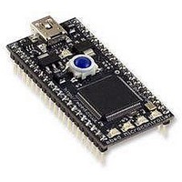
Manufacturer Part Number
OM11042,598
Description
Microcontroller Modules & Accessories mbed LPC2368 Demo Board
Manufacturer
NXP Semiconductors
Datasheet
1.OM11042598.pdf
(59 pages)
Specifications of OM11042,598
Product
Microcontroller Modules
Data Bus Width
32 bit
Core Processor
LPC2368
Clock Speed
60 MHz
Interface Type
Ethernet, CAN, I2C, SPI, UART
Operating Supply Voltage
3 V to 3.6 V
Lead Free Status / RoHS Status
Lead free / RoHS Compliant


NXP Semiconductors
LPC2364_65_66_67_68_6
Product data sheet
7.8 Fast general purpose parallel I/O
Device pins that are not connected to a specific peripheral function are controlled by the
GPIO registers. Pins may be dynamically configured as inputs or outputs. Separate
registers allow setting or clearing any number of outputs simultaneously. The value of the
output register may be read back as well as the current state of the port pins.
LPC2364/65/66/67/68 use accelerated GPIO functions:
•
•
•
•
•
•
•
•
•
•
•
•
•
•
•
•
•
•
Single DMA and burst DMA request signals. Each peripheral connected to the
GPDMA can assert either a burst DMA request or a single DMA request. The DMA
burst size is set by programming the GPDMA.
Memory-to-memory, memory-to-peripheral, peripheral-to-memory, and
peripheral-to-peripheral transfers.
Scatter or gather DMA is supported through the use of linked lists. This means that
the source and destination areas do not have to occupy contiguous areas of memory.
Hardware DMA channel priority. Each DMA channel has a specific hardware priority.
DMA channel 0 has the highest priority and channel 1 has the lowest priority. If
requests from two channels become active at the same time the channel with the
highest priority is serviced first.
AHB slave DMA programming interface. The GPDMA is programmed by writing to the
DMA control registers over the AHB slave interface.
One AHB master for transferring data. This interface transfers data when a DMA
request goes active.
32-bit AHB master bus width.
Incrementing or non-incrementing addressing for source and destination.
Programmable DMA burst size. The DMA burst size can be programmed to more
efficiently transfer data. Usually the burst size is set to half the size of the FIFO in the
peripheral.
Internal four-word FIFO per channel.
Supports 8-bit, 16-bit, and 32-bit wide transactions.
An interrupt to the processor can be generated on a DMA completion or when a DMA
error has occurred.
Interrupt masking. The DMA error and DMA terminal count interrupt requests can be
masked.
Raw interrupt status. The DMA error and DMA count raw interrupt status can be read
prior to masking.
GPIO registers are relocated to the ARM local bus so that the fastest possible I/O
timing can be achieved.
Mask registers allow treating sets of port bits as a group, leaving other bits
unchanged.
All GPIO registers are byte and half-word addressable.
Entire port value can be written in one instruction.
Rev. 06 — 1 February 2010
LPC2364/65/66/67/68
Single-chip 16-bit/32-bit microcontrollers
© NXP B.V. 2010. All rights reserved.
20 of 59
Related parts for OM11042,598
Image
Part Number
Description
Manufacturer
Datasheet
Request
R

Part Number:
Description:
DEVELOPMENT BOARD FOR LPC2368
Manufacturer:
NXP Semiconductors
Datasheet:

Part Number:
Description:
NXP Semiconductors designed the LPC2420/2460 microcontroller around a 16-bit/32-bitARM7TDMI-S CPU core with real-time debug interfaces that include both JTAG andembedded trace
Manufacturer:
NXP Semiconductors
Datasheet:

Part Number:
Description:
NXP Semiconductors designed the LPC2458 microcontroller around a 16-bit/32-bitARM7TDMI-S CPU core with real-time debug interfaces that include both JTAG andembedded trace
Manufacturer:
NXP Semiconductors
Datasheet:
Part Number:
Description:
NXP Semiconductors designed the LPC2468 microcontroller around a 16-bit/32-bitARM7TDMI-S CPU core with real-time debug interfaces that include both JTAG andembedded trace
Manufacturer:
NXP Semiconductors
Datasheet:
Part Number:
Description:
NXP Semiconductors designed the LPC2470 microcontroller, powered by theARM7TDMI-S core, to be a highly integrated microcontroller for a wide range ofapplications that require advanced communications and high quality graphic displays
Manufacturer:
NXP Semiconductors
Datasheet:
Part Number:
Description:
NXP Semiconductors designed the LPC2478 microcontroller, powered by theARM7TDMI-S core, to be a highly integrated microcontroller for a wide range ofapplications that require advanced communications and high quality graphic displays
Manufacturer:
NXP Semiconductors
Datasheet:
Part Number:
Description:
The Philips Semiconductors XA (eXtended Architecture) family of 16-bit single-chip microcontrollers is powerful enough to easily handle the requirements of high performance embedded applications, yet inexpensive enough to compete in the market for hi
Manufacturer:
NXP Semiconductors
Datasheet:
Part Number:
Description:
The XA-S3 device is a member of Philips Semiconductors? XA(eXtended Architecture) family of high performance 16-bitsingle-chip microcontrollers
Manufacturer:
NXP Semiconductors
Datasheet:

Part Number:
Description:
The NXP BlueStreak LH75401/LH75411 family consists of two low-cost 16/32-bit System-on-Chip (SoC) devices
Manufacturer:
NXP Semiconductors
Datasheet:
Part Number:
Description:
The NXP LPC3130/3131 combine an 180 MHz ARM926EJ-S CPU core, high-speed USB2
Manufacturer:
NXP Semiconductors
Datasheet:
Part Number:
Description:
The NXP LPC3141 combine a 270 MHz ARM926EJ-S CPU core, High-speed USB 2
Manufacturer:
NXP Semiconductors
Part Number:
Description:
The NXP LPC3143 combine a 270 MHz ARM926EJ-S CPU core, High-speed USB 2
Manufacturer:
NXP Semiconductors

Part Number:
Description:
The NXP LPC3152 combines an 180 MHz ARM926EJ-S CPU core, High-speed USB 2
Manufacturer:
NXP Semiconductors
Part Number:
Description:
The NXP LPC3154 combines an 180 MHz ARM926EJ-S CPU core, High-speed USB 2
Manufacturer:
NXP Semiconductors