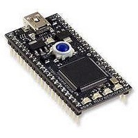
OM11042,598 NXP Semiconductors, OM11042,598 Datasheet - Page 12

OM11042,598
Manufacturer Part Number
OM11042,598
Description
Microcontroller Modules & Accessories mbed LPC2368 Demo Board
Manufacturer
NXP Semiconductors
Datasheet
1.OM11042598.pdf
(59 pages)
Specifications of OM11042,598
Product
Microcontroller Modules
Data Bus Width
32 bit
Core Processor
LPC2368
Clock Speed
60 MHz
Interface Type
Ethernet, CAN, I2C, SPI, UART
Operating Supply Voltage
3 V to 3.6 V
Lead Free Status / RoHS Status
Lead free / RoHS Compliant
NXP Semiconductors
Table 4.
LPC2364_65_66_67_68_6
Product data sheet
Symbol
P1[20]/PWM1[2]/
SCK0
P1[21]/PWM1[3]/
SSEL0
P1[22]/MAT1[0]
P1[23]/PWM1[4]/
MISO0
P1[24]/PWM1[5]/
MOSI0
P1[25]/MAT1[1]
P1[26]/PWM1[6]/
CAP0[0]
P1[27]/CAP0[1]
P1[28]/
PCAP1[0]/
MAT0[0]
P1[29]/
PCAP1[1]/
MAT0[1]
P1[30]/V
AD0[4]
P1[31]/SCK1/
AD0[5]
P2[0] to P2[31]
P2[0]/PWM1[1]/
TXD1/
TRACECLK
BUS
Pin description
/
Pin
34
35
36
37
38
39
40
43
44
45
21
20
75
[1]
[1]
[1]
[1]
[1]
[1]
[1]
[1]
[1]
[1]
[2]
[2]
[1]
…continued
Ball
K4
F5
J5
K5
H5
G5
K6
K7
J7
G6
H1
F4
B9
[1]
[1]
[1]
[2]
[1]
[1]
[1]
[1]
[1]
[1]
[2]
[1]
[1]
Type
I/O
O
I/O
I/O
O
I/O
I/O
O
I/O
O
I/O
I/O
O
I/O
I/O
O
I/O
O
I
I/O
I
I/O
I
O
I/O
I
O
I/O
I
I
I/O
I/O
I
I/O
I/O
O
O
O
Description
P1[20] — General purpose digital input/output pin.
PWM1[2] — Pulse Width Modulator 1, channel 2 output.
SCK0 — Serial clock for SSP0.
P1[21] — General purpose digital input/output pin.
PWM1[3] — Pulse Width Modulator 1, channel 3 output.
SSEL0 — Slave Select for SSP0.
P1[22] — General purpose digital input/output pin.
MAT1[0] — Match output for Timer 1, channel 0.
P1[23] — General purpose digital input/output pin.
PWM1[4] — Pulse Width Modulator 1, channel 4 output.
MISO0 — Master In Slave Out for SSP0.
P1[24] — General purpose digital input/output pin.
PWM1[5] — Pulse Width Modulator 1, channel 5 output.
MOSI0 — Master Out Slave in for SSP0.
P1[25] — General purpose digital input/output pin.
MAT1[1] — Match output for Timer 1, channel 1.
P1[26] — General purpose digital input/output pin.
PWM1[6] — Pulse Width Modulator 1, channel 6 output.
CAP0[0] — Capture input for Timer 0, channel 0.
P1[27] — General purpose digital input/output pin.
CAP0[1] — Capture input for Timer 0, channel 1.
P1[28] — General purpose digital input/output pin.
PCAP1[0] — Capture input for PWM1, channel 0.
MAT0[0] — Match output for Timer 0, channel 0.
P1[29] — General purpose digital input/output pin.
PCAP1[1] — Capture input for PWM1, channel 1.
MAT0[1] — Match output for Timer 0, channel 0.
P1[30] — General purpose digital input/output pin.
V
Note: This signal must be HIGH for USB reset to occur.
AD0[4] — A/D converter 0, input 4.
P1[31] — General purpose digital input/output pin.
SCK1 — Serial Clock for SSP1.
AD0[5] — A/D converter 0, input 5.
Port 2: Port 2 is a 32-bit I/O port with individual direction controls for each
bit. The operation of Port 2 pins depends upon the pin function selected via
the pin connect block. Pins 14 through 31 of this port are not available.
P2[0] — General purpose digital input/output pin.
PWM1[1] — Pulse Width Modulator 1, channel 1 output.
TXD1 — Transmitter output for UART1.
TRACECLK — Trace Clock.
Rev. 06 — 1 February 2010
BUS
— Monitors the presence of USB bus power. (LPC2364/66/68 only)
LPC2364/65/66/67/68
Single-chip 16-bit/32-bit microcontrollers
© NXP B.V. 2010. All rights reserved.
12 of 59


