OM11042,598 NXP Semiconductors, OM11042,598 Datasheet - Page 14
OM11042,598
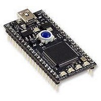
Manufacturer Part Number
OM11042,598
Description
Microcontroller Modules & Accessories mbed LPC2368 Demo Board
Manufacturer
NXP Semiconductors
Datasheet
1.OM11042598.pdf
(59 pages)
Specifications of OM11042,598
Product
Microcontroller Modules
Data Bus Width
32 bit
Core Processor
LPC2368
Clock Speed
60 MHz
Interface Type
Ethernet, CAN, I2C, SPI, UART
Operating Supply Voltage
3 V to 3.6 V
Lead Free Status / RoHS Status
Lead free / RoHS Compliant


NXP Semiconductors
Table 4.
LPC2364_65_66_67_68_6
Product data sheet
Symbol
P2[11]/EINT1/
MCIDAT1/
I2STX_CLK
P2[12]/EINT2/
MCIDAT2/
I2STX_WS
P2[13]/EINT3/
MCIDAT3/
I2STX_SDA
P3[0] to P3[31]
P3[25]/MAT0[0]/
PWM1[2]
P3[26]/MAT0[1]/
PWM1[3]
P4[0] to P4[31]
P4[28]/MAT2[0]/
TXD3
P4[29]/MAT2[1]/
RXD3
DBGEN
TDO
TDI
TMS
TRST
Pin description
Pin
52
51
50
27
26
82
85
-
1
2
3
4
[1]
[1]
[1]
[1]
[6]
[6]
[6]
[1]
[1]
[1]
[1]
…continued
Ball
H8
K10
J9
H3
K1
C7
E6
D4
A1
C3
B1
C2
[6]
[1]
[1]
[1]
[1]
[6]
[1]
[1]
[1]
[1]
[1]
[6]
Type
I/O
I
O
I/O
I/O
I
O
I/O
I/O
I
O
I/O
I/O
I/O
O
O
I/O
O
O
I/O
I/O
O
O
I/O
O
I
I
O
I
I
I
Description
P2[11] — General purpose digital input/output pin.
EINT1 — External interrupt 1 input.
MCIDAT1 — Data line for SD/MMC interface. (LPC2367/68 only)
I2STX_CLK — Transmit Clock. It is driven by the master and received by
the slave. Corresponds to the signal SCK in the I
P2[12] — General purpose digital input/output pin.
EINT2 — External interrupt 2 input.
MCIDAT2 — Data line for SD/MMC interface. (LPC2367/68 only)
I2STX_WS — Transmit Word Select. It is driven by the master and
received by the slave. Corresponds to the signal WS in the I
specification.
P2[13] — General purpose digital input/output pin.
EINT3 — External interrupt 3 input.
MCIDAT3 — Data line for SD/MMC interface. (LPC2367/68 only)
I2STX_SDA — Transmit data. It is driven by the transmitter and read by the
receiver. Corresponds to the signal SD in the I
Port 3: Port 3 is a 32-bit I/O port with individual direction controls for each
bit. The operation of Port 3 pins depends upon the pin function selected via
the pin connect block. Pins 0 through 24, and 27 through 31 of this port are
not available.
P3[25] — General purpose digital input/output pin.
MAT0[0] — Match output for Timer 0, channel 0.
PWM1[2] — Pulse Width Modulator 1, output 2.
P3[26] — General purpose digital input/output pin.
MAT0[1] — Match output for Timer 0, channel 1.
PWM1[3] — Pulse Width Modulator 1, output 3.
Port 4: Port 4 is a 32-bit I/O port with individual direction controls for each
bit. The operation of Port 4 pins depends upon the pin function selected via
the pin connect block. Pins 0 through 27, 30, and 31 of this port are not
available.
P4[28] — General purpose digital input/output pin.
MAT2[0] — Match output for Timer 2, channel 0.
TXD3 — Transmitter output for UART3.
P4[29] — General purpose digital input/output pin.
MAT2[1] — Match output for Timer 2, channel 1.
RXD3 — Receiver input for UART3.
DBGEN — JTAG interface control signal. Also used for boundary scanning.
Note: This pin is available in LPC2364FET100 and LPC2368FET100
devices only (TFBGA package).
TDO — Test Data out for JTAG interface.
TDI — Test Data in for JTAG interface.
TMS — Test Mode Select for JTAG interface.
TRST — Test Reset for JTAG interface.
Rev. 06 — 1 February 2010
LPC2364/65/66/67/68
Single-chip 16-bit/32-bit microcontrollers
2
S-bus specification.
2
S-bus specification.
© NXP B.V. 2010. All rights reserved.
2
S-bus
14 of 59
Related parts for OM11042,598
Image
Part Number
Description
Manufacturer
Datasheet
Request
R

Part Number:
Description:
DEVELOPMENT BOARD FOR LPC2368
Manufacturer:
NXP Semiconductors
Datasheet:

Part Number:
Description:
NXP Semiconductors designed the LPC2420/2460 microcontroller around a 16-bit/32-bitARM7TDMI-S CPU core with real-time debug interfaces that include both JTAG andembedded trace
Manufacturer:
NXP Semiconductors
Datasheet:

Part Number:
Description:
NXP Semiconductors designed the LPC2458 microcontroller around a 16-bit/32-bitARM7TDMI-S CPU core with real-time debug interfaces that include both JTAG andembedded trace
Manufacturer:
NXP Semiconductors
Datasheet:
Part Number:
Description:
NXP Semiconductors designed the LPC2468 microcontroller around a 16-bit/32-bitARM7TDMI-S CPU core with real-time debug interfaces that include both JTAG andembedded trace
Manufacturer:
NXP Semiconductors
Datasheet:
Part Number:
Description:
NXP Semiconductors designed the LPC2470 microcontroller, powered by theARM7TDMI-S core, to be a highly integrated microcontroller for a wide range ofapplications that require advanced communications and high quality graphic displays
Manufacturer:
NXP Semiconductors
Datasheet:
Part Number:
Description:
NXP Semiconductors designed the LPC2478 microcontroller, powered by theARM7TDMI-S core, to be a highly integrated microcontroller for a wide range ofapplications that require advanced communications and high quality graphic displays
Manufacturer:
NXP Semiconductors
Datasheet:
Part Number:
Description:
The Philips Semiconductors XA (eXtended Architecture) family of 16-bit single-chip microcontrollers is powerful enough to easily handle the requirements of high performance embedded applications, yet inexpensive enough to compete in the market for hi
Manufacturer:
NXP Semiconductors
Datasheet:
Part Number:
Description:
The XA-S3 device is a member of Philips Semiconductors? XA(eXtended Architecture) family of high performance 16-bitsingle-chip microcontrollers
Manufacturer:
NXP Semiconductors
Datasheet:

Part Number:
Description:
The NXP BlueStreak LH75401/LH75411 family consists of two low-cost 16/32-bit System-on-Chip (SoC) devices
Manufacturer:
NXP Semiconductors
Datasheet:
Part Number:
Description:
The NXP LPC3130/3131 combine an 180 MHz ARM926EJ-S CPU core, high-speed USB2
Manufacturer:
NXP Semiconductors
Datasheet:
Part Number:
Description:
The NXP LPC3141 combine a 270 MHz ARM926EJ-S CPU core, High-speed USB 2
Manufacturer:
NXP Semiconductors
Part Number:
Description:
The NXP LPC3143 combine a 270 MHz ARM926EJ-S CPU core, High-speed USB 2
Manufacturer:
NXP Semiconductors

Part Number:
Description:
The NXP LPC3152 combines an 180 MHz ARM926EJ-S CPU core, High-speed USB 2
Manufacturer:
NXP Semiconductors
Part Number:
Description:
The NXP LPC3154 combines an 180 MHz ARM926EJ-S CPU core, High-speed USB 2
Manufacturer:
NXP Semiconductors