OM6271 NXP Semiconductors, OM6271 Datasheet - Page 7
OM6271
Manufacturer Part Number
OM6271
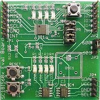
Description
Interface Modules & Development Tools SPI to I2C Master Bridge Demoboard
Manufacturer
NXP Semiconductors
Datasheet
1.OM6271.pdf
(30 pages)
Specifications of OM6271
Interface Type
I2C, SPI
Data Bus Width
8 bit
For Use With/related Products
SC18IS601IPW
Lead Free Status / RoHS Status
Lead free / RoHS Compliant


NXP Semiconductors
SC18IS600_601_5
Product data sheet
6.2.1.1 Quasi-bidirectional output configuration
Quasi-bidirectional outputs can be used both as an input and output without the need to
reconfigure the pin. This is possible because when the pin outputs a logic HIGH, it is
weakly driven, allowing an external device to pull the pin LOW. When the pin is driven
LOW, it is driven strongly and able to sink a large current. There are three pull-up
transistors in the quasi-bidirectional output that serve different purposes.
One of these pull-ups, called the ‘very weak’ pull-up, is turned on whenever the pin latch
for the pin contains a logic 1. This very weak pull-up sources a very small current that will
pull the pin HIGH if it is left floating.
A second pull-up, called the ‘weak’ pull-up, is turned on when the pin latch for the pin
contains a logic 1 and the pin itself is also at a logic 1 level. This pull-up provides the
primary source current for a quasi-bidirectional pin that is outputting a 1. If this pin is
pulled LOW by an external device, the weak pull-up turns off, and only the very weak
pull-up remains on. In order to pull the pin LOW under these conditions, the external
device has to sink enough current to overpower the weak pull-up and pull the pin below its
input threshold voltage.
The third pull-up is referred to as the ‘strong’ pull-up. This pull-up is used to speed up
LOW-to-HIGH transitions on a quasi-bidirectional pin when the pin latch changes from a
logic 0 to a logic 1. When this occurs, the strong pull-up turns on for two system clock
cycles quickly pulling the pin HIGH.
The quasi-bidirectional pin configuration is shown in
Although the SC18IS600/601 is a 3 V device, most of the pins are 5 V tolerant. If 5 V is
applied to a pin configured in quasi-bidirectional mode, there will be a current flowing from
the pin to V
configured in quasi-bidirectional mode is discouraged.
A quasi-bidirectional pin has a Schmitt-triggered input that also has a glitch suppression
circuit.
Fig 6.
pin latch data
Quasi-bidirectional output configuration
DD
causing extra power consumption. Therefore, applying 5 V to pins
Rev. 05 — 28 July 2008
2 SYSTEM
CYCLES
CLOCK
P
input data
V
SS
strong
Figure
P
SC18IS600/601
6.
very
weak
SPI to I
P
glitch rejection
weak
© NXP B.V. 2008. All rights reserved.
2
V
C-bus interface
DD
002aab882
GPIOn,
IOn pin
7 of 30
Related parts for OM6271
Image
Part Number
Description
Manufacturer
Datasheet
Request
R

Part Number:
Description:
NXP Semiconductors designed the LPC2420/2460 microcontroller around a 16-bit/32-bitARM7TDMI-S CPU core with real-time debug interfaces that include both JTAG andembedded trace
Manufacturer:
NXP Semiconductors
Datasheet:

Part Number:
Description:
NXP Semiconductors designed the LPC2458 microcontroller around a 16-bit/32-bitARM7TDMI-S CPU core with real-time debug interfaces that include both JTAG andembedded trace
Manufacturer:
NXP Semiconductors
Datasheet:
Part Number:
Description:
NXP Semiconductors designed the LPC2468 microcontroller around a 16-bit/32-bitARM7TDMI-S CPU core with real-time debug interfaces that include both JTAG andembedded trace
Manufacturer:
NXP Semiconductors
Datasheet:
Part Number:
Description:
NXP Semiconductors designed the LPC2470 microcontroller, powered by theARM7TDMI-S core, to be a highly integrated microcontroller for a wide range ofapplications that require advanced communications and high quality graphic displays
Manufacturer:
NXP Semiconductors
Datasheet:
Part Number:
Description:
NXP Semiconductors designed the LPC2478 microcontroller, powered by theARM7TDMI-S core, to be a highly integrated microcontroller for a wide range ofapplications that require advanced communications and high quality graphic displays
Manufacturer:
NXP Semiconductors
Datasheet:
Part Number:
Description:
The Philips Semiconductors XA (eXtended Architecture) family of 16-bit single-chip microcontrollers is powerful enough to easily handle the requirements of high performance embedded applications, yet inexpensive enough to compete in the market for hi
Manufacturer:
NXP Semiconductors
Datasheet:
Part Number:
Description:
The XA-S3 device is a member of Philips Semiconductors? XA(eXtended Architecture) family of high performance 16-bitsingle-chip microcontrollers
Manufacturer:
NXP Semiconductors
Datasheet:

Part Number:
Description:
The NXP BlueStreak LH75401/LH75411 family consists of two low-cost 16/32-bit System-on-Chip (SoC) devices
Manufacturer:
NXP Semiconductors
Datasheet:
Part Number:
Description:
The NXP LPC3130/3131 combine an 180 MHz ARM926EJ-S CPU core, high-speed USB2
Manufacturer:
NXP Semiconductors
Datasheet:
Part Number:
Description:
The NXP LPC3141 combine a 270 MHz ARM926EJ-S CPU core, High-speed USB 2
Manufacturer:
NXP Semiconductors
Part Number:
Description:
The NXP LPC3143 combine a 270 MHz ARM926EJ-S CPU core, High-speed USB 2
Manufacturer:
NXP Semiconductors

Part Number:
Description:
The NXP LPC3152 combines an 180 MHz ARM926EJ-S CPU core, High-speed USB 2
Manufacturer:
NXP Semiconductors
Part Number:
Description:
The NXP LPC3154 combines an 180 MHz ARM926EJ-S CPU core, High-speed USB 2
Manufacturer:
NXP Semiconductors

Part Number:
Description:
Standard level N-channel enhancement mode Field-Effect Transistor (FET) in a plastic package using NXP High-Performance Automotive (HPA) TrenchMOS technology
Manufacturer:
NXP Semiconductors
Datasheet: