OM6271 NXP Semiconductors, OM6271 Datasheet - Page 6
OM6271
Manufacturer Part Number
OM6271
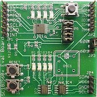
Description
Interface Modules & Development Tools SPI to I2C Master Bridge Demoboard
Manufacturer
NXP Semiconductors
Datasheet
1.OM6271.pdf
(30 pages)
Specifications of OM6271
Interface Type
I2C, SPI
Data Bus Width
8 bit
For Use With/related Products
SC18IS601IPW
Lead Free Status / RoHS Status
Lead free / RoHS Compliant


NXP Semiconductors
6. Functional description
Table 3.
[1]
[2]
SC18IS600_601_5
Product data sheet
Register
address
0x00
0x01
0x02
0x03
0x04
0x05
For SC18IS601, these bits are ‘Don’t care’.
For SC18IS601 GPIO3 is not used.
Register
IOConfig
IOState
I2CClock
I2CTO
I2CStat
I2CAdr
Internal registers summary
6.2.1 Programmable IO port configuration register (IOConfig)
6.1 Internal registers
6.2 Register descriptions
Bit 7
IO3.1
0
CR7
TO6
1
ADR7
The SC18IS600/601 acts as a bridge between a SPI interface and an I
SPI master device to communicate with I
Mode 3 of the SPI specification and can operate up to 3 Mbit/s (SC18IS601).
The SC18IS600/601 provides internal registers for monitoring and control. These
registers are shown in
paragraphs.
Pins GPIO0 to GPIO3 may be configured by software to one of four types. These are:
quasi-bidirectional, push-pull, open-drain, and input-only. Two configuration bits per pin,
located in the IOConfig register, select the IO type for each pin. Each pin has
Schmitt-triggered input that also has a glitch suppression circuit. IO4 and IO5 are
quasi-bidirectional pins and are not user-configurable. For SC18IS601, GPIO3 is
non-existent.
Table 4
correspond to GPIOx.
Table 4.
IOx.1
0
0
1
1
[1]
Bit 6
IO3.0
0
CR6
TO5
1
ADR6
shows the configurations for the programmable I/O pins. IOx.1 and IOx.0
Pin configurations
[1]
IOx.0
0
1
0
1
Bit 5
IO2.1
GPIO5
CR5
TO4
1
ADR5
Table
Pin configuration
quasi-bidirectional output configuration
input-only configuration
push-pull output configuration
open-drain output configuration
Rev. 05 — 28 July 2008
Bit 4
IO2.0
GPIO4
CR4
TO3
1
ADR4
3. Register functions are more fully described in the following
Bit 3
IO1.1
GPIO3
CR3
TO2
I2CSTAT3 I2CSTAT2 I2CSTAT1 I2CSTAT0 R
ADR3
[2]
2
C-bus slave devices. The SPI interface supports
Bit 2
IO1.0
GPIO2
CR2
TO1
ADR2
Bit 1
IO0.1
GPIO1
CR1
TO0
ADR1
SC18IS600/601
SPI to I
Bit 0
IO0.0
GPIO0
CR0
TE
X
2
© NXP B.V. 2008. All rights reserved.
C-bus. It allows a
2
C-bus interface
R/W
R/W
R/W
R/W
R/W
R/W
Default
value
0x00
0x3F
0x19
0xFE
0xF0
0x00
6 of 30
Related parts for OM6271
Image
Part Number
Description
Manufacturer
Datasheet
Request
R

Part Number:
Description:
NXP Semiconductors designed the LPC2420/2460 microcontroller around a 16-bit/32-bitARM7TDMI-S CPU core with real-time debug interfaces that include both JTAG andembedded trace
Manufacturer:
NXP Semiconductors
Datasheet:

Part Number:
Description:
NXP Semiconductors designed the LPC2458 microcontroller around a 16-bit/32-bitARM7TDMI-S CPU core with real-time debug interfaces that include both JTAG andembedded trace
Manufacturer:
NXP Semiconductors
Datasheet:
Part Number:
Description:
NXP Semiconductors designed the LPC2468 microcontroller around a 16-bit/32-bitARM7TDMI-S CPU core with real-time debug interfaces that include both JTAG andembedded trace
Manufacturer:
NXP Semiconductors
Datasheet:
Part Number:
Description:
NXP Semiconductors designed the LPC2470 microcontroller, powered by theARM7TDMI-S core, to be a highly integrated microcontroller for a wide range ofapplications that require advanced communications and high quality graphic displays
Manufacturer:
NXP Semiconductors
Datasheet:
Part Number:
Description:
NXP Semiconductors designed the LPC2478 microcontroller, powered by theARM7TDMI-S core, to be a highly integrated microcontroller for a wide range ofapplications that require advanced communications and high quality graphic displays
Manufacturer:
NXP Semiconductors
Datasheet:
Part Number:
Description:
The Philips Semiconductors XA (eXtended Architecture) family of 16-bit single-chip microcontrollers is powerful enough to easily handle the requirements of high performance embedded applications, yet inexpensive enough to compete in the market for hi
Manufacturer:
NXP Semiconductors
Datasheet:
Part Number:
Description:
The XA-S3 device is a member of Philips Semiconductors? XA(eXtended Architecture) family of high performance 16-bitsingle-chip microcontrollers
Manufacturer:
NXP Semiconductors
Datasheet:

Part Number:
Description:
The NXP BlueStreak LH75401/LH75411 family consists of two low-cost 16/32-bit System-on-Chip (SoC) devices
Manufacturer:
NXP Semiconductors
Datasheet:
Part Number:
Description:
The NXP LPC3130/3131 combine an 180 MHz ARM926EJ-S CPU core, high-speed USB2
Manufacturer:
NXP Semiconductors
Datasheet:
Part Number:
Description:
The NXP LPC3141 combine a 270 MHz ARM926EJ-S CPU core, High-speed USB 2
Manufacturer:
NXP Semiconductors
Part Number:
Description:
The NXP LPC3143 combine a 270 MHz ARM926EJ-S CPU core, High-speed USB 2
Manufacturer:
NXP Semiconductors

Part Number:
Description:
The NXP LPC3152 combines an 180 MHz ARM926EJ-S CPU core, High-speed USB 2
Manufacturer:
NXP Semiconductors
Part Number:
Description:
The NXP LPC3154 combines an 180 MHz ARM926EJ-S CPU core, High-speed USB 2
Manufacturer:
NXP Semiconductors

Part Number:
Description:
Standard level N-channel enhancement mode Field-Effect Transistor (FET) in a plastic package using NXP High-Performance Automotive (HPA) TrenchMOS technology
Manufacturer:
NXP Semiconductors
Datasheet: