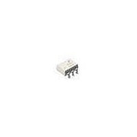
MOC3052M Fairchild Semiconductor, MOC3052M Datasheet - Page 8

MOC3052M
Manufacturer Part Number
MOC3052M
Description
Triac & SCR Output Optocouplers DIP-6 NON-ZERO TRIAC
Manufacturer
Fairchild Semiconductor
Datasheet
1.MOC3052M_F132.pdf
(13 pages)
Specifications of MOC3052M
Configuration
1
Maximum Input Current
50 mA
Maximum Operating Temperature
+ 100 C
Maximum Power Dissipation
330 mW
Maximum Reverse Diode Voltage
6 V
Minimum Operating Temperature
- 40 C
Output Type
AC
Package / Case
PDIP White
Typical Input Voltage
1.2 V
Zero-crossing Circuit
No
Output Device
Triac
Isolation Voltage
5000 Vrms
Peak Output Voltage (vdrm)
600 V
Maximum Input Voltage
1.4 V
Maximum Output Voltage
420 VAC
Minimum Trigger Current
10 mA (Max)
Lead Free Status / RoHS Status
Lead free / RoHS Compliant
Other names
MOC3052M_NL
Available stocks
Company
Part Number
Manufacturer
Quantity
Price
Company:
Part Number:
MOC3052M
Manufacturer:
FSC
Quantity:
10 000
Company:
Part Number:
MOC3052M
Manufacturer:
FAIRCHIL
Quantity:
432
Part Number:
MOC3052M
Manufacturer:
FAIRCHILD/仙童
Quantity:
20 000
Company:
Part Number:
MOC3052M-A
Manufacturer:
MAXIM
Quantity:
5 037
Part Number:
MOC3052M/CT3052
Manufacturer:
FAIRCHILD/仙童
Quantity:
20 000
©2005 Fairchild Semiconductor Corporation
MOC3051M, MOC3052M Rev. 1.0.5
CONTROL
Applications Guide
Basic Triac Driver Circuit
The new random phase triac driver family MOC3052M
and MOC3051M are very immune to static dv/dt which
allows snubberless operations in all applications where
external generated noise in the AC line is below its guar-
anteed dv/dt withstand capability. For these applications
a snubber circuit is not necessary when a noise insensi-
tive power triac is used. Figure 11 shows the circuit
diagram. The triac driver is directly connected to the triac
main terminal 2 and a series Resistor R which limits the
current to the triac driver. Current limiting resistor R must
have a minimum value which restricts the current into the
driver to maximum 1A.
R = Vp AC/I
The power dissipation of this current limiting resistor and
the triac driver is very small because the power triac
carries the load current as soon as the current through
driver and current limiting resistor reaches the trigger
current of the power triac. The switching transition times
for the driver is only one micro second and for power
triacs typical four micro seconds.
V CC
RET .
R LED
Figure 11. Basic Driver Circuit
TM
Q
max rep. = Vp AC/1A
TRIAC DRIVER
R LED = (V CC - V F LED - V sat Q)/I FT
R = V p AC line/I TSM
Figure 13. Triac Driver Circuit for Extremely Noisy Environments
CONTROL
V CC
RET.
R
POWER TRIAC
R LED
Recommended snubber to pass IEEE472 and IEC255-4 noise tests
R S = 47 , C S = 0.01 F
TRIAC DRIVER
LOAD
AC LINE
8
R
POWER TRIAC
Triac Driver Circuit for Noisy Environments
When the transient rate of rise and amplitude are
expected to exceed the power triacs and triac drivers
maximum ratings a snubber circuit as shown in Figure
12 is recommended. Fast transients are slowed by the
R-C snubber and excessive amplitudes are clipped by
the Metal Oxide Varistor MOV.
Triac Driver Circuit for Extremely Noisy
Environments
As specified in the noise
IEC255-4.
Industrial control applications do specify a maximum
transient noise dv/dt and peak voltage which is super-
imposed onto the AC line voltage. In order to pass this
environment noise test a modified snubber network as
shown in Figure 13 is recommended.
CONTROL
Figure 12. Triac Driver Circuit for Noisy Environments
V CC
RET.
R LED
R S
Typical Snubber values R S = 33 , C S = 0.01 F
MOV (Metal Oxide Varistor) protects triac and
driver from transient overvoltages >V DRM max.
C S
TRIAC DRIVER
MOV
LOAD
AC LINE
R
POWER TRIAC
standards IEEE472 and
R S
C S
www.fairchildsemi.com
MOV
LOAD
AC LINE


