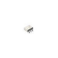
MOC3052M Fairchild Semiconductor, MOC3052M Datasheet - Page 7

MOC3052M
Manufacturer Part Number
MOC3052M
Description
Triac & SCR Output Optocouplers DIP-6 NON-ZERO TRIAC
Manufacturer
Fairchild Semiconductor
Datasheet
1.MOC3052M_F132.pdf
(13 pages)
Specifications of MOC3052M
Configuration
1
Maximum Input Current
50 mA
Maximum Operating Temperature
+ 100 C
Maximum Power Dissipation
330 mW
Maximum Reverse Diode Voltage
6 V
Minimum Operating Temperature
- 40 C
Output Type
AC
Package / Case
PDIP White
Typical Input Voltage
1.2 V
Zero-crossing Circuit
No
Output Device
Triac
Isolation Voltage
5000 Vrms
Peak Output Voltage (vdrm)
600 V
Maximum Input Voltage
1.4 V
Maximum Output Voltage
420 VAC
Minimum Trigger Current
10 mA (Max)
Lead Free Status / RoHS Status
Lead free / RoHS Compliant
Other names
MOC3052M_NL
Available stocks
Company
Part Number
Manufacturer
Quantity
Price
Company:
Part Number:
MOC3052M
Manufacturer:
FSC
Quantity:
10 000
Company:
Part Number:
MOC3052M
Manufacturer:
FAIRCHIL
Quantity:
432
Part Number:
MOC3052M
Manufacturer:
FAIRCHILD/仙童
Quantity:
20 000
Company:
Part Number:
MOC3052M-A
Manufacturer:
MAXIM
Quantity:
5 037
Part Number:
MOC3052M/CT3052
Manufacturer:
FAIRCHILD/仙童
Quantity:
20 000
©2005 Fairchild Semiconductor Corporation
MOC3051M, MOC3052M Rev. 1.0.5
t(delay), t(f) versus I
The triac driver’s turn on switching speed consists of a
turn on delay time t(d) and a fall time t(f). Figure 9 shows
that the delay time depends on the LED trigger current,
while the actual trigger transition time t(f) stays constant
with about one micro second.
The delay time is important in very short pulsed opera-
tion because it demands a higher trigger current at very
short trigger pulses. This dependency is shown in the
graph I
The turn on transition time t(f) combined with the power
triac’s turn on time is important to the power dissipation
of this device.
ISOL. TRANSF.
0.1
AC
10
1
10
FT
Figure 9. Delay Time, t(d), and Fall Time, t(f),
vs. LED PW.
Switching Time Test Circuit
10k
I
V TM
20
FT
I FT
- LED TRIGGER CURRENT (mA)
t(d)
V TM
vs. LED Trigger Current
SCOPE
t(f)
DUT
30
FT
t f
t d
I FT
100
40
ZERO CROSS
GENERATOR
DETECTOR
FUNCTION
EXT . SYNC
V out
50
115 VAC
PHASE CTRL.
PW CTRL.
PERIOD CTRL.
V o AMPL. CTRL.
60
APPLIED VOLTAGE
WAVEFORM
7
0 VOLTS
1. The mercury wetted relay provides a high speed
2. 100x scope probes are used, to allow high speeds and
3. The worst-case condition for static dv/dt is established
PULSE
INPUT
+400
Vdc
repeated pulse to the D.U.T.
voltages.
by triggering the D.U.T. with a normal LED input
current, then removing the current. The variable R
allows the dv/dt to be gradually increased until the
D.U.T. continues to trigger in response to the applied
voltage pulse, even after the LED current has been
removed. The dv/dt is then decreased until the D.U.T.
stops triggering.
recorded.
MERCURY
WETTED
RELAY
252V
Figure 10. Static dv/dt Test Circuit
RC
R
RC
TEST
is measured at this point and
C TEST
D.U.T.
R = 1k
dv/dt =
V max = 400V
SCOPE
PROBE
X100
www.fairchildsemi.com
0.63V
RC
TEST
=
252
RC


