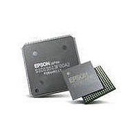
S1D13743F00A200 Epson, S1D13743F00A200 Datasheet - Page 31

S1D13743F00A200
Manufacturer Part Number
S1D13743F00A200
Description
LCD Drivers LCD CNTRL w/Embedded 464KB SRAM
Manufacturer
Epson
Datasheet
1.S1D13743F00A200.pdf
(134 pages)
Specifications of S1D13743F00A200
Maximum Clock Frequency
33 MHz, 68.59 MHz
Operating Supply Voltage
1.5 V
Maximum Operating Temperature
+ 85 C
Package / Case
QFP-20-144
Attached Touch Screen
No
Maximum Supply Current
74 mA
Minimum Operating Temperature
- 40 C
Lead Free Status / RoHS Status
Lead free / RoHS Compliant
Available stocks
Company
Part Number
Manufacturer
Quantity
Price
Company:
Part Number:
S1D13743F00A200
Manufacturer:
EPSON
Quantity:
5 690
- Current page: 31 of 134
- Download datasheet (3Mb)
Epson Research and Development
Vancouver Design Center
Hardware Functional Specification
Issue Date: 2010/05/18
MD[15:0]
(Note 4)
Signal
D/C#
WE#
CS#
RD#
Symbol
t
t
t
t
t
t
t
t
t
codh
t
t
t
t
t
t
t
rodh
t
wah
t
crdz
wcs
t
t
rrdz
w2r
r2w
t
t
ast
rah
rcs
dst
dht
rdv
rdd
csf
wc
wh
t
ch
wl
rc
rh
rl
Address setup time (read/write)
Address hold time (write)
Address hold time (read)
Chip Select setup time (write)
Chip Select setup time (read)
Chip Select hold time (read/write)
Chip Select Wait time (read/write)
Register Write cycle
LUT write cycle
Memory write cycle
Pulse low duration
Pulse high duration
WR# rising edge to RD# falling edge
RD# rising edge to WR# falling edge
Read cycle
Pulse low duration
Pulse high duration for Registers
Pulse high duration for Memory and LUT
Write data setup time
Write data hold time
Read data hold time from RD# rising edge
RD# rising edge to MD High-Z
Read data hold time from CS# rising edge
CS# rising edge to MD High-Z
RD# falling edge to MD valid for Registers
RD# falling edge to MD valid for LUT
RD# falling edge to MD valid for Memory
RD# falling edge to MD valid for Registers
RD# falling edge to MD valid for LUT
RD# falling edge to MD valid for Memory
RD# falling edge to MD driven
RD# falling edge to MD driven
Note
1. For a read cycle after a write cycle, MD[15:0] must be driven Hi-Z a maximum
2. For a write cycle after a read cycle, MD[15:0] should not be driven by the host
3. Assumes CS# remains low. After the rising edge of RD#, if CS# goes high
4. When CNF1=0, only MD[7:0] are used. When CNF1=1, MD[7:0] are used for all
Table 7-5: Intel 80 Input A.C. Characteristics - 3.3 Volt
of t
until t
before t
accesses except for the Memory Data Port when MD[15:0] are used.
rdd
Parameter
rrdz
after the falling edge of RD#.
rrdz
after the rising edge of RD#.
then MD[15:0] will go to High-Z according to t
Revision 2.7
1SYSCLK + 26
2SYSCLK + 2
2SYSCLK + 2
t
t
wc
rl
Min
t
0.5
31
10
12
27
36
11
t
—
—
—
—
—
—
—
—
+ t
rdv
t
2
6
0
1
5
2
7
3
2
wl
rl
- t
rh
wl
4SYSCLK + 22
5SYSCLK + 15
4SYSCLK + 19
5SYSCLK + 12
Max
—
—
31
12
10
—
—
—
—
—
—
—
—
—
—
—
—
—
—
—
—
—
—
—
—
—
—
8
crdz
.
Unit
ns
ns
ns
ns
ns
ns
ns
ns
ns
ns
ns
ns
ns
ns
ns
ns
ns
ns
ns
ns
ns
ns
ns
ns
ns
ns
ns
ns
ns
ns
ns
ns
Description
CL=30pF
CL = 8pF
CL=30pF
CL = 8pF
X70A-A-001-02
Note 1
Note 2
Note 3
S1D13743
Page 31
Related parts for S1D13743F00A200
Image
Part Number
Description
Manufacturer
Datasheet
Request
R

Part Number:
Description:
Display Modules & Development Tools S1D13743 Eval board
Manufacturer:
Epson

Part Number:
Description:
INK CARTRIDGE, T0803, EPSON, MAG
Manufacturer:
Epson
Datasheet:

Part Number:
Description:
INK CARTRIDGE, T0804, EPSON, YEL
Manufacturer:
Epson
Datasheet:

Part Number:
Description:
CXA1034M
Manufacturer:
EPSON Electronics
Datasheet:

Part Number:
Description:
Manufacturer:
EPSON Electronics
Datasheet:

Part Number:
Description:
Manufacturer:
EPSON Electronics
Datasheet:

Part Number:
Description:
Manufacturer:
EPSON Electronics
Datasheet:

Part Number:
Description:
Manufacturer:
EPSON Electronics
Datasheet:

Part Number:
Description:
RTC58321Real time clock module(4-bit I/O CONNECTION REAL TIME CLOCK MODULE)
Manufacturer:
EPSON Electronics
Datasheet:

Part Number:
Description:
SCI7661DC-DC Converter
Manufacturer:
EPSON Electronics
Datasheet:

Part Number:
Description:
Manufacturer:
EPSON Electronics
Datasheet:

Part Number:
Description:
Manufacturer:
EPSON Electronics
Datasheet:


