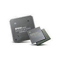
S1D13743F00A200 Epson, S1D13743F00A200 Datasheet - Page 120

S1D13743F00A200
Manufacturer Part Number
S1D13743F00A200
Description
LCD Drivers LCD CNTRL w/Embedded 464KB SRAM
Manufacturer
Epson
Datasheet
1.S1D13743F00A200.pdf
(134 pages)
Specifications of S1D13743F00A200
Maximum Clock Frequency
33 MHz, 68.59 MHz
Operating Supply Voltage
1.5 V
Maximum Operating Temperature
+ 85 C
Package / Case
QFP-20-144
Attached Touch Screen
No
Maximum Supply Current
74 mA
Minimum Operating Temperature
- 40 C
Lead Free Status / RoHS Status
Lead free / RoHS Compliant
Available stocks
Company
Part Number
Manufacturer
Quantity
Price
Company:
Part Number:
S1D13743F00A200
Manufacturer:
EPSON
Quantity:
5 690
- Current page: 120 of 134
- Download datasheet (3Mb)
Page 120
22 PLL Power Supply Considerations
22.1 Guidelines for PLL Power Layout
S1D13743
X70A-A-001-02
Notes:
•
•
•
PLLVDD and PLLVSS traces should be as short as possible
PLLVDD and PLLVSS must be separated from the digital supply
Digital power and ground to L1 and L2 should be short parallel traces
on the same side of the board to reduce any loop area that can induce noise
Regulator
Voltage
The PLL circuit is an analog circuit which is very sensitive to noise on the input clock
waveform or the power supply. Noise on the clock or the supplied power may cause the
operation of the PLL circuit to become unstable or increase the jitter.
Due to these noise constraints, it is highly recommended that the power supply traces or the
power plane for the PLL be isolated from those of other power supplies. Filtering should
also be used to keep the power as clean as possible.
The following are guidelines which, if followed, will result in cleaner power to the PLL,
this will result in a cleaner and more stable clock. Even a partial implementation of these
guidelines will give results.
The PLL circuit is an analog circuit and is very sensitive to noise on the input clock
waveform or the power supply. Noise on the clock or the supplied power may cause the
operation of the PLL circuit to become unstable or increase the jitter.
Due to these noise constraints, it is highly recommended that the power supply traces or the
power plane for the PLL be isolated from those of other power supplies. Filtering should
also be used to keep the power as clean as possible.
The following are guidelines which, if followed, will result in cleaner power to the PLL,
resulting in a cleaner and more stable clock. Even a partial implementation of these guide-
lines will give results.
PLL power traces
must split from the
digital traces very
close to the regulator
To Digital V
To Digital IOV
Figure 22-1: PLL Power Layout
SS
Plane
DD
Plane
Revision 2.7
Optional, but recommended
C3
L1
L2
C2
C1
PLLV
PLLV
Typical Values:
L1, L2
C1
C2
C3
Actual values may be different and
subject to validation
Epson Research and Development
Hardware Functional Specification
DD
SS
isolation bead
~10uf bypass
1nf bypass
.1uf bypass
Vancouver Design Center
S1D13743
Issue Date: 2010/05/18
Related parts for S1D13743F00A200
Image
Part Number
Description
Manufacturer
Datasheet
Request
R

Part Number:
Description:
Display Modules & Development Tools S1D13743 Eval board
Manufacturer:
Epson

Part Number:
Description:
INK CARTRIDGE, T0803, EPSON, MAG
Manufacturer:
Epson
Datasheet:

Part Number:
Description:
INK CARTRIDGE, T0804, EPSON, YEL
Manufacturer:
Epson
Datasheet:

Part Number:
Description:
CXA1034M
Manufacturer:
EPSON Electronics
Datasheet:

Part Number:
Description:
Manufacturer:
EPSON Electronics
Datasheet:

Part Number:
Description:
Manufacturer:
EPSON Electronics
Datasheet:

Part Number:
Description:
Manufacturer:
EPSON Electronics
Datasheet:

Part Number:
Description:
Manufacturer:
EPSON Electronics
Datasheet:

Part Number:
Description:
RTC58321Real time clock module(4-bit I/O CONNECTION REAL TIME CLOCK MODULE)
Manufacturer:
EPSON Electronics
Datasheet:

Part Number:
Description:
SCI7661DC-DC Converter
Manufacturer:
EPSON Electronics
Datasheet:

Part Number:
Description:
Manufacturer:
EPSON Electronics
Datasheet:

Part Number:
Description:
Manufacturer:
EPSON Electronics
Datasheet:


