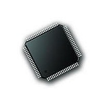
PIC18F87J72-I/PT Microchip Technology, PIC18F87J72-I/PT Datasheet - Page 444

PIC18F87J72-I/PT
Manufacturer Part Number
PIC18F87J72-I/PT
Description
IC PIC MCU 8BIT 14KB FLSH 80TQFP
Manufacturer
Microchip Technology
Series
PIC® 18Fr
Datasheet
1.PIC18F86J72-IPT.pdf
(480 pages)
Specifications of PIC18F87J72-I/PT
Program Memory Type
FLASH
Program Memory Size
128KB (64K x 16)
Package / Case
80-TQFP
Core Processor
PIC
Core Size
8-Bit
Speed
48MHz
Connectivity
I²C, LIN, SPI, UART/USART
Peripherals
Brown-out Detect/Reset, LCD, LVD, POR, PWM, WDT
Number Of I /o
51
Ram Size
3.8K x 8
Voltage - Supply (vcc/vdd)
2 V ~ 3.6 V
Data Converters
A/D 12x12b
Oscillator Type
Internal
Operating Temperature
-40°C ~ 85°C
Data Bus Width
8 bit
Data Ram Size
4 KB
Interface Type
SPI, USART, SPI, I2C
Maximum Clock Frequency
8 MHz
Number Of Programmable I/os
51
Number Of Timers
4
Operating Supply Voltage
2 V to 3.6 V
Maximum Operating Temperature
+ 85 C
Mounting Style
SMD/SMT
Minimum Operating Temperature
- 40 C
On-chip Adc
14
Controller Family/series
PIC18F
No. Of I/o's
51
Ram Memory Size
3923Byte
Cpu Speed
48MHz
No. Of Timers
4
Rohs Compliant
Yes
Lead Free Status / RoHS Status
Lead free / RoHS Compliant
Lead Free Status / RoHS Status
Lead free / RoHS Compliant, Lead free / RoHS Compliant
Available stocks
Company
Part Number
Manufacturer
Quantity
Price
Company:
Part Number:
PIC18F87J72-I/PT
Manufacturer:
Microchip
Quantity:
210
Company:
Part Number:
PIC18F87J72-I/PT
Manufacturer:
Microchip Technology
Quantity:
10 000
- Current page: 444 of 480
- Download datasheet (5Mb)
PIC18F87J72 FAMILY
B.4.3
B.4.3.1
Both of the ADCs in the AFE are identical and they
include a second-order modulator with a multi-bit DAC
architecture (see Figure B-2). The quantizer is a Flash
ADC composed of 4 comparators with equally spaced
thresholds and a thermometer output coding. The
proprietary 5-level architecture ensures minimum
quantization noise at the outputs of the modulators
without disturbing linearity or inducing additional
distortion. The sampling frequency is DMCLK (typically
1 MHz with MCLK = 4 MHz) so the modulator outputs
are refreshed at a DMCLK rate.
Both modulators also include a dithering algorithm that
can be enabled through the DITHER<1:0> bits in the
Configuration register. This dithering process improves
THD and SFDR (for high OSR settings) while
increasing slightly the noise floor of the ADCs. For
power metering applications and applications that are
distortion-sensitive, it is recommended to keep
DITHER enabled for both ADCs. In the case of power
metering applications, THD and SFDR are critical
specifications to optimize SNR (noise floor). This is not
really problematic due to the large averaging factor at
the output of the ADCs; therefore, even for low OSR
settings, the dithering algorithm will show a positive
impact on the performance of the application.
Figure B-2 represents a simplified block diagram of the
Delta-Sigma ADC present on the AFE.
FIGURE B-2:
DS39979A-page 444
Voltage Input
Differential
DELTA-SIGMA MODULATOR
Architecture
Delta-Sigma Modulator
SIMPLIFIED DELTA-SIGMA
ADC BLOCK DIAGRAM
Loop
Filter
Integrator
Second
Order
Flash ADC
DAC
Quantizer
5-Level
Output
Bitstream
Preliminary
B.4.3.2
For a specified voltage reference value of 2.4V, the mod-
ulators’ specified differential input range is ±500 mV. The
input range is proportional to V
to the V
the modulator over amplitude and frequency. Outside of
this range, the modulator is still functional, however, its
stability is no longer ensured, and therefore, it is not rec-
ommended to exceed this limit. The saturation point for
the modulator is V
ADC includes a gain of 3 by default (independent from
the PGA setting). See Section B.4.5 “ADC Output
Coding”.
B.4.3.3
The
independent Boost mode for each channel. If the
corresponding BOOST<1:0> bit is enabled, the power
consumption of the modulator is multiplied by 2 and its
bandwidth is increased to be able to sustain AMCLK
clock frequencies, up to 8.192 MHz, while keeping the
ADC accuracy. When disabled, the power consumption
is back to normal and the AMCLK clock frequencies
can only reach up to 5 MHz without affecting ADC
accuracy.
B.4.4
Both of the ADCs include a decimation filter that is a
third-order sinc (or notch) filter. This filter processes the
multi-bit bitstream into 16 or 24-bit words (depending
on the WIDTH Configuration bit). The settling time of
the filter is 3 DMCLK periods. It is recommended to dis-
card unsettled data to avoid data corruption, which can
be done easily by setting the DR_LTY bit high in the
STATUS/COM register.
The resolution achievable at the output of the sinc filter
(the output of the ADC) is dependant on the OSR and
is summarized with the following table:
TABLE B-5:
For 24-Bit Output mode (WIDTH = 1), the output of the
sinc filter is padded with least significant zeros for any
resolution less than 24 bits.
For 16-Bit Output modes, the output of the sinc filter is
rounded to the closest 16-bit number in order to
conserve only 16-bit words and to minimize truncation
error.
OSR<1:0>
0
0
1
1
Delta-Sigma
REF
0
1
0
1
SINC
voltage. This range ensures the stability of
Modulator Input Range and
Saturation Point
Boost Mode
REF
3
ADC RESOLUTION vs. OSR
FILTER
OSR
/3 since the transfer function of the
128
256
modulators
32
64
2010 Microchip Technology Inc.
REF
ADC Resolution (bits)
No Missing Codes
and scales according
also
17
20
23
24
include
an
Related parts for PIC18F87J72-I/PT
Image
Part Number
Description
Manufacturer
Datasheet
Request
R

Part Number:
Description:
Manufacturer:
Microchip Technology Inc.
Datasheet:

Part Number:
Description:
Manufacturer:
Microchip Technology Inc.
Datasheet:

Part Number:
Description:
Manufacturer:
Microchip Technology Inc.
Datasheet:

Part Number:
Description:
Manufacturer:
Microchip Technology Inc.
Datasheet:

Part Number:
Description:
Manufacturer:
Microchip Technology Inc.
Datasheet:

Part Number:
Description:
Manufacturer:
Microchip Technology Inc.
Datasheet:

Part Number:
Description:
Manufacturer:
Microchip Technology Inc.
Datasheet:

Part Number:
Description:
Manufacturer:
Microchip Technology Inc.
Datasheet:


