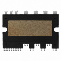
FSBB15CH60C Fairchild Semiconductor, FSBB15CH60C Datasheet - Page 13
FSBB15CH60C
Manufacturer Part Number
FSBB15CH60C
Description
IC POWER MOD SPM 600V SPM27CC
Manufacturer
Fairchild Semiconductor
Series
SPM™r
Type
IGBTr
Specifications of FSBB15CH60C
Configuration
3 Phase
Current
15A
Voltage
600V
Voltage - Isolation
2500Vrms
Package / Case
SPM27CC
Transistor Polarity
N Channel
Dc Collector Current
15A
Collector Emitter Voltage Vces
2V
Power Dissipation Pd
55W
Collector Emitter Voltage V(br)ceo
600V
Operating Temperature Range
-40°C To
Operating Temperature (max)
150C
Operating Temperature (min)
-40C
Pin Count
27
Mounting
Through Hole
Case Length
44mm
Case Height
5.5mm
Screening Level
Automotive
Lead Free Status / RoHS Status
Lead free / RoHS Compliant
Available stocks
Company
Part Number
Manufacturer
Quantity
Price
Company:

Part Number:
FSBB15CH60C
Manufacturer:
CYPRESS
Quantity:
5 610
Part Number:
FSBB15CH60C
Manufacturer:
FSC/ON可看货
Quantity:
20 000


FSBB15CH60C Rev. D
Note:
1) To avoid malfunction, the wiring of each input should be as short as possible. (less than 2-3cm)
2) By virtue of integrating an application specific type HVIC inside the SPM, direct coupling to CPU terminals without any opto-coupler or transformer isolation is possible.
3) V
4) C
5) V
6) Input signal is High-Active type. There is a 5k Ω resistor inside the IC to pull down each input signal line to GND. RC coupling circuits should be adopted for the prevention of
7) To prevent errors of the protection function, the wiring around R
8) In the short-circuit protection circuit, please select the R
9) Each capacitor should be mounted as close to the pins of the SPM as possible.
10) To prevent surge destruction, the wiring between the smoothing capacitor and the P&GND pins should be as short as possible. The use of a high frequency non-inductive
11) Relays are used at almost every systems of electrical equipments of home appliances. In these cases, there should be sufficient distance between the CPU and the relays.
12) C
input signal oscillation. R
(typ.)) Please refer to the note 5 for calculation method.
C
U
P
FO
FO
capacitor of around 0.1~0.22 μ F between the P&GND pins is recommended.
SP15
SPC15
output is open collector type. This signal line should be pulled up to the positive side of the 5V power supply with approximately 4.7k Ω resistance. Please refer to Figure11.
output pulse width should be determined by connecting an external capacitor(C
of around 7 times larger than bootstrap capacitor C
Gating W H
Gating W L
Gating VH
Gating UH
Gating VL
Gating UL
should be over 1 μ F and mounted as close to the pins of the SPM as possible.
Fault
Short-Circuit Protection
Input Signal for
C
BPF
R
R
R
R
R
R
R
S
S
S
S
S
S
S
S
C
C
PS
PS
C
time constant should be selected in the range 50~150ns
PS
C
C
C
C
PS
PS
PS
PS
5V line
R
C
PF
PF
15V line
Figure 13. Typical Application Circuit
F
C
BS
SC
R
F
C
is recommended.
time constant in the range 1.5~2 μ s.
SP15
F
and C
C
C
C
C
BS
BS
BS
SC
C
SPC15
SC
C
C
C
BSC
BSC
BSC
C
should be as short as possible.
FOD
(13) IN
(9) IN
(12) V
(19) V
(18) V
(17) IN
(20) V
(15) V
(14) V
(16) V
(11) V
(10) V
W-Phase Current
U-Phase Current
V-Phase Current
(7) C
(6) V
(4) IN
(1) V
(8) C
(5) IN
(3) IN
(2) COM
13
(UH)
S(U)
B(W )
CC(H)
S(W )
B(V)
CC(H)
B(U)
CC(H)
FO
CC(L)
S(V)
SC
FOD
FOD
(VH)
(VL)
(W H)
(W L)
(UL)
.
) between C
C
PS
should not be less than 1nF.
VB
VCC
COM
IN
VB
VCC
COM
VB
VCC
COM
IN
C(SC)
C(FOD)
VFO
IN(W L)
IN(VL)
IN(UL)
COM
VCC
IN
FOD
OUT(W L)
OUT(VL)
OUT(UL)
(pin7) and COM(pin2). (Example : if C
OUT
OUT
OUT
V
VS
VS
VS
SL
C
FW
C
FV
(
Recommended R
C
FU
R
R
N
R
N
N
P (27)
W (26)
V (25)
U (24)
FW
W
V
FV
U
FU
(22)
(21)
(23)
S
=100 Ω , C
FOD
= 33 nF, then t
R
R
R
PS
SW
SV
SU
M
=1nF)
www.fairchildsemi.com
C
DCS
FO
= 1.8ms
Vdc
Related parts for FSBB15CH60C
Image
Part Number
Description
Manufacturer
Datasheet
Request
R

Part Number:
Description:
Fairchild Semiconductor [IGBT MODULE]
Manufacturer:
Fairchild Semiconductor
Datasheet:

Part Number:
Description:
Discrete Semiconductor Modules
Manufacturer:
Fairchild Semiconductor
Part Number:
Description:
Discrete Semiconductor Modules
Manufacturer:
Fairchild Semiconductor
Part Number:
Description:
This N-Channel MOSFET is produced using Fairchild Semiconductor’s advanced Power Trench® process
Manufacturer:
Fairchild Semiconductor
Datasheet:
Part Number:
Description:
This N-Channel MOSFET is produced using Fairchild Semiconductor’s advanced Power Trench® process
Manufacturer:
Fairchild Semiconductor
Datasheet:
Part Number:
Description:
This N-Channel MOSFET is produced using Fairchild Semiconductor’s advanced PowerTrench® process
Manufacturer:
Fairchild Semiconductor
Datasheet:
Part Number:
Description:
This N-Channel MOSFET is produced using Fairchild Semiconductor’s advanced PowerTrench® process
Manufacturer:
Fairchild Semiconductor
Datasheet:
Part Number:
Description:
This N-Channel MOSFET is produced using Fairchild Semiconductor’s advanced Power Trench® process
Manufacturer:
Fairchild Semiconductor
Datasheet:
Part Number:
Description:
This N-Channel logic Level MOSFETs are produced using Fairchild Semiconductor‘s advanced Power Trench® process that has been special tailored to minimize the on-state resistance and yet maintain superior switching performance
Manufacturer:
Fairchild Semiconductor
Datasheet:
Part Number:
Description:
This N-Channel MOSFET is produced using Fairchild Semiconductor’s advanced Power Trench® process
Manufacturer:
Fairchild Semiconductor
Datasheet:
Part Number:
Description:
This N-Channel SyncFET™ is produced using Fairchild Semiconductor’s advanced PowerTrench® process
Manufacturer:
Fairchild Semiconductor
Datasheet:
Part Number:
Description:
This N-Channel SyncFET™ is produced using Fairchild Semiconductor’s advanced PowerTrench® process
Manufacturer:
Fairchild Semiconductor
Datasheet:
Part Number:
Description:
This N-Channel SyncFET™ is produced using Fairchild Semiconductor’s advanced PowerTrench® process
Manufacturer:
Fairchild Semiconductor
Datasheet:
Part Number:
Description:
This N-Channel logic Level MOSFETs are produced using Fairchild Semiconductor‘s advanced Power Trench® process that has been special tailored to minimize the on-state resistance and yet maintain superior switching performance
Manufacturer:
Fairchild Semiconductor
Datasheet:
Part Number:
Description:
This N-Channel MOSFET is produced using Fairchild Semiconductor’s advanced Power Trench® process that has been especially tailored to minimize the on-state resistance and yet maintain superior switching performance
Manufacturer:
Fairchild Semiconductor
Datasheet: