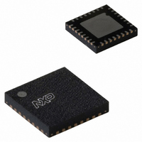
MFRC52301HN1,157 NXP Semiconductors, MFRC52301HN1,157 Datasheet - Page 19

MFRC52301HN1,157
Manufacturer Part Number
MFRC52301HN1,157
Description
IC READER 13.56MHZ 32-HVQFN
Manufacturer
NXP Semiconductors
Datasheet
1.MFRC52301HN1151.pdf
(97 pages)
Specifications of MFRC52301HN1,157
Frequency
13.56MHz
Package / Case
32-VQFN Exposed Pad, 32-HVQFN, 32-SQFN, 32-DHVQFN
Lead Free Status / RoHS Status
Lead free / RoHS Compliant
Features
-
Rf Type
-
Lead Free Status / RoHS Status
Lead free / RoHS Compliant
Other names
935282956157
- Current page: 19 of 97
- Download datasheet (3Mb)
NXP Semiconductors
MFRC523_34
Product data sheet
PUBLIC
8.3.4.5 7-Bit addressing
8.3.4.6 Register write access
During the I
determine which slave will be selected by the master.
Several address numbers are reserved. During device configuration, the designer must
ensure that collisions with these reserved addresses cannot occur. Check the I
specification for a complete list of reserved addresses.
The I
after releasing pin NRSTPD or after a power-on reset, the device defines the I
address according to pin EA.
If pin EA is set LOW, the upper 4 bits of the device bus address are reserved by
NXP Semiconductors and set to 0101b for all MFRC523 devices. The remaining 3 bits
(ADR_0, ADR_1, ADR_2) of the slave address can be freely configured by the customer
to prevent collisions with other I
If pin EA is set HIGH, ADR_0 to ADR_5 can be completely specified at the external pins
according to
In both modes, the external address coding is latched immediately after releasing the
reset condition. Further changes at the used pins are not taken into consideration.
Depending on the external wiring, the I
outputs.
To write data from the host controller using the I
MFRC523 the following frame format must be used.
In one frame, all data bytes are written to the same register address. This enables fast
FIFO buffer access. The Read/Write (R/W) bit is set to logic 0.
Fig 16. First byte following the START procedure
•
•
The first byte of a frame indicates the device address according to the I
The second byte indicates the register address followed by up to n-data bytes.
2
C-bus address specification is dependent on the definition of pin EA. Immediately
2
C-bus address procedure, the first byte after the START condition is used to
Table 5 on page
All information provided in this document is subject to legal disclaimers.
MSB
bit 6
Rev. 3.5 — 24 September 2010
bit 5
10. ADR_6 is always set to logic 0.
115235
2
bit 4
C-bus devices.
slave address
2
C-bus address pins can be used for test signal
bit 3
bit 2
2
C-bus to a specific register in the
bit 1
bit 0
Contactless reader IC
001aak591
LSB
R/W
MFRC523
© NXP B.V. 2010. All rights reserved.
2
C-bus rules.
2
2
C-bus
C-bus
19 of 97
Related parts for MFRC52301HN1,157
Image
Part Number
Description
Manufacturer
Datasheet
Request
R
Part Number:
Description:
Manufacturer:
NXP Semiconductors
Datasheet:
Part Number:
Description:
NXP Semiconductors designed the LPC2420/2460 microcontroller around a 16-bit/32-bitARM7TDMI-S CPU core with real-time debug interfaces that include both JTAG andembedded trace
Manufacturer:
NXP Semiconductors
Datasheet:

Part Number:
Description:
NXP Semiconductors designed the LPC2458 microcontroller around a 16-bit/32-bitARM7TDMI-S CPU core with real-time debug interfaces that include both JTAG andembedded trace
Manufacturer:
NXP Semiconductors
Datasheet:
Part Number:
Description:
NXP Semiconductors designed the LPC2468 microcontroller around a 16-bit/32-bitARM7TDMI-S CPU core with real-time debug interfaces that include both JTAG andembedded trace
Manufacturer:
NXP Semiconductors
Datasheet:
Part Number:
Description:
NXP Semiconductors designed the LPC2470 microcontroller, powered by theARM7TDMI-S core, to be a highly integrated microcontroller for a wide range ofapplications that require advanced communications and high quality graphic displays
Manufacturer:
NXP Semiconductors
Datasheet:
Part Number:
Description:
NXP Semiconductors designed the LPC2478 microcontroller, powered by theARM7TDMI-S core, to be a highly integrated microcontroller for a wide range ofapplications that require advanced communications and high quality graphic displays
Manufacturer:
NXP Semiconductors
Datasheet:
Part Number:
Description:
The Philips Semiconductors XA (eXtended Architecture) family of 16-bit single-chip microcontrollers is powerful enough to easily handle the requirements of high performance embedded applications, yet inexpensive enough to compete in the market for hi
Manufacturer:
NXP Semiconductors
Datasheet:
Part Number:
Description:
The XA-S3 device is a member of Philips Semiconductors? XA(eXtended Architecture) family of high performance 16-bitsingle-chip microcontrollers
Manufacturer:
NXP Semiconductors
Datasheet:

Part Number:
Description:
The NXP BlueStreak LH75401/LH75411 family consists of two low-cost 16/32-bit System-on-Chip (SoC) devices
Manufacturer:
NXP Semiconductors
Datasheet:

Part Number:
Description:
The NXP LPC3130/3131 combine an 180 MHz ARM926EJ-S CPU core, high-speed USB2
Manufacturer:
NXP Semiconductors
Datasheet:

Part Number:
Description:
The NXP LPC3141 combine a 270 MHz ARM926EJ-S CPU core, High-speed USB 2
Manufacturer:
NXP Semiconductors

Part Number:
Description:
The NXP LPC3143 combine a 270 MHz ARM926EJ-S CPU core, High-speed USB 2
Manufacturer:
NXP Semiconductors

Part Number:
Description:
The NXP LPC3152 combines an 180 MHz ARM926EJ-S CPU core, High-speed USB 2
Manufacturer:
NXP Semiconductors

Part Number:
Description:
The NXP LPC3154 combines an 180 MHz ARM926EJ-S CPU core, High-speed USB 2
Manufacturer:
NXP Semiconductors


