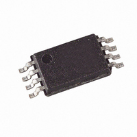
T48C862M-R4-TNQ Atmel, T48C862M-R4-TNQ Datasheet - Page 7

T48C862M-R4-TNQ
Manufacturer Part Number
T48C862M-R4-TNQ
Description
IC MON TIRE PRESS 433MHZ 24-SOIC
Manufacturer
Atmel
Datasheet
1.T48C862M-R4-TNS.pdf
(107 pages)
Specifications of T48C862M-R4-TNQ
Frequency
433MHz
Modulation Or Protocol
FM, FSK
Data Rate - Maximum
32 kBaud
Power - Output
10dBm
Current - Transmitting
9.5mA
Data Interface
PCB, Surface Mount
Antenna Connector
PCB, Surface Mount
Memory Size
1KB EEPROM, 1KB RAM
Voltage - Supply
2 V ~ 4 V
Operating Temperature
-40°C ~ 125°C
Package / Case
24-SOIC (0.200", 5.30mm Width)
Lead Free Status / RoHS Status
Contains lead / RoHS non-compliant
Features
-
Applications
-
CLK Output
Clock Pulse Take Over
Output Matching and Power
Setting
4551C–4BMCU–01/04
Figure 4. Tolerances of Frequency Modulation
Using C
capacitances on each side of the crystal of C
capacitance of the crystal of C
FSK deviation of ±21 kHz typical with worst case tolerances of ±16.3 kHz to ±28.8 kHz
results.
An output CLK signal is provided for a connected microcontroller. The delivered signal is
CMOS compatible if the load capacitance is lower than 10 pF.
The clock of the crystal oscillator can be used for clocking the microcontroller. the micro-
controller block has the special feature of starting with an integrated RC-oscillator to
switch on the PLL transmitter block with ENABLE = H, and after 1 ms to assume the
clock signal of the transmission IC, so the message can be sent with crystal accuracy.
The output power is set by the load impedance of the antenna. The maximum output
power is achieved with a load impedance of Z
low resistive path to V
The delivered current pulse of the power amplifier is 9 mA and the maximum output
power is delivered to a resistive load of 465
power amplifier is compensated by the load impedance.
An optimum load impedance of:
Z
power of 7.5 dBm.
The load impedance is defined as the impedance seen from the PLL transmitter block’s
ANT1, ANT2 into the matching network. Do not confuse this large signal load imped-
ance with a small signal input impedance delivered as input characteristic of RF
amplifiers and measured from the application into the IC instead of from the IC into the
application for a power amplifier.
Less output power is achieved by lowering the real parallel part of 465
parallel imaginary part should be kept constant.
Output power measurement can be done with the circuit shown in Figure 5 on page 8.
Note that the component values must be changed to compensate the individual board
p a r a s i t i c s u n t i l t h e P L L t r a n s m i t t e r b l o c k h a s t h e r i g h t l o a d i m p e d a n c e
Z
power must be calibrated.
Load
Load,opt
= 465
4
= (166 + j223) . Also the damping of the cable used to measure the output
= 9.2 pF ±2%, C
|| j/(2
XTAL
V
S
S
~
to deliver the DC current.
1.0 pF) = (166 + j223)
5
= 6.8 pF ±5%, a switch port with C
0
C
= 3.2 pF ±10% and a crystal with C
Stray1
T48C862-R4 [Preliminary]
Crystal equivalent circuit
C
M
L
C
M
0
Load,opt
if the 1.0 pF output capacitance of the
Stray1
R
S
thus results for the maximum output
= (166 + j223) . There must be a
= C
Stray2
C
Stray2
C
5
= 1 pF ±10%, a parallel
Switch
C
Switch
C
4
= 3 pF ±10%, stray
M
= 13 fF ±10%, an
where the
7


