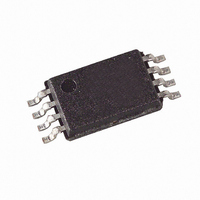
T48C862M-R4-TNQ Atmel, T48C862M-R4-TNQ Datasheet - Page 59

T48C862M-R4-TNQ
Manufacturer Part Number
T48C862M-R4-TNQ
Description
IC MON TIRE PRESS 433MHZ 24-SOIC
Manufacturer
Atmel
Datasheet
1.T48C862M-R4-TNS.pdf
(107 pages)
Specifications of T48C862M-R4-TNQ
Frequency
433MHz
Modulation Or Protocol
FM, FSK
Data Rate - Maximum
32 kBaud
Power - Output
10dBm
Current - Transmitting
9.5mA
Data Interface
PCB, Surface Mount
Antenna Connector
PCB, Surface Mount
Memory Size
1KB EEPROM, 1KB RAM
Voltage - Supply
2 V ~ 4 V
Operating Temperature
-40°C ~ 125°C
Package / Case
24-SOIC (0.200", 5.30mm Width)
Lead Free Status / RoHS Status
Contains lead / RoHS non-compliant
Features
-
Applications
-
Timer 3 – Mode 7:
Carrier Frequency Burst
Modulation Controlled by SSI
Internal Output (SO)
Timer 3 – Mode 8:
FSK Modulation with Shift
Register Data (SO)
Timer 3 – Mode 9:
Pulse-width Modulation with
the Shift Register
4551C–4BMCU–01/04
The Timer 3 counter is driven by an internal or external clock source. Its compare- and
compare mode registers must be programmed to generate the carrier frequency via the
output toggle flip-flop. The output (SO) of the SSI is used to enable or disable the Timer
3 output. The SSI should be supplied with the toggle signal of Timer 2 (see “Combina-
tion Mode 12: Burst Modulation 2” on page 88).
The two compare registers are used for generating two different time intervals. The SSI
internal data output (SO) selects which compare register is used for the output fre-
quency generation. A "0" level at the SSI data output enables the compare register 1. A
"1" level enables compare register 2. The compare- and compare-mode registers must
be programmed to generate the two frequencies via the output toggle flip-flop. The SSI
can be supplied with the toggle signal of Timer 2. The Timer 3 counter is driven by an
internal or external clock source. The Timer 2 counter is driven by the Counter 3 (TOG3)
(see “Combination Mode 13: FSK Modulation” on page 88).
Figure 57. FSK Modulation
The two compare registers are used for generating two different time intervals. The SSI
internal data output (SO) selects which compare register is used for the output pulse
generation. In this mode both compare- and compare-mode registers must be pro-
grammed for generating the two pulse widths. It is also useful to enable the single-action
mode for extreme duty cycles. Timer 2 is used as baudrate generator and for the trigger
restart of Timer 3. The SSI must be supplied with a toggle signal of Timer 2. The counter
is driven by an internal or external clock source (see “Combination Mode 7: Pulse-width
Modulation (PWM)” on page 83).
Figure 58. Pulse-width Modulation
Counter 3
Counter 3
CM31
CM32
TOG2
CM31
CM32
T3O
SCO
T3R
T3R
T3O
SIR
SO
SO
0 0 0 0 0 0 0 0 0
0 1 2 3 4 0 1 2 3 4 0 1 2 3
0
0
0 0 0 0
0
0 0 0 0 0 1 2 3 4 5 6 7 8 9 1011121314150 1 2 3 4 5
T48C862-R4 [Preliminary]
4 0 1 2 0 1 2 0 1 2 0 1 2 0 1 2 0 1 2 0 1 2 0 1 2 3
1
1
6 7 8
0
9
10
1112
13
14
15
0
0
4 0
1
2 3
1
1
4
59


