RXM-GPS-SG-T Linx Technologies Inc, RXM-GPS-SG-T Datasheet - Page 15
RXM-GPS-SG-T
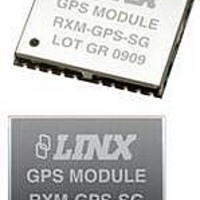
Manufacturer Part Number
RXM-GPS-SG-T
Description
GPS MODULE SMD SIRF
Manufacturer
Linx Technologies Inc
Series
SGr
Type
GPS Moduler
Datasheet
1.MDEV-GPS-SG.pdf
(17 pages)
Specifications of RXM-GPS-SG-T
Package / Case
Module
Operating Voltage
4.2 V
Operating Current
46 mA
Frequency Range
1575.42 MHz
Interface Type
UART, USB
Operating Temperature Range
- 30 C to + 85 C
Lead Free Status / RoHS Status
Lead free / RoHS Compliant
Features
-
Voltage - Supply
-
Frequency
-
Operating Temperature
-
Applications
-
Sensitivity
-
Memory Size
-
Data Interface
-
Data Rate - Maximum
-
Modulation Or Protocol
-
Antenna Connector
-
Current - Receiving
-
Lead Free Status / Rohs Status
Lead free / RoHS Compliant


BOARD LAYOUT GUIDELINES
Page 28
Page 28
The module’s design makes integration straightforward; however, it is still critical
to exercise care in PCB layout. Failure to observe good layout techniques can
result in a significant degradation of the module’s performance. A primary layout
goal is to maintain a characteristic 50-ohm impedance throughout the path from
the antenna to the module. Grounding, filtering, decoupling, routing and PCB
stack-up are also important considerations for any RF design. The following
section provides some basic design guidelines which may be helpful.
During prototyping, the module should be soldered to a properly laid-out circuit
board. The use of prototyping or “perf” boards will result in poor performance and
is strongly discouraged.
The module should, as much as reasonably possible, be isolated from other
components on your PCB, especially high-frequency circuitry such as crystal
oscillators, switching power supplies, and high-speed bus lines.
When possible, separate RF and digital circuits into different PCB regions. Make
sure internal wiring is routed away from the module and antenna, and is secured
to prevent displacement.
Do not route PCB traces directly under the module. There should not be any
copper or traces under the module on the same layer as the module, just bare
PCB. The underside of the module has traces and vias that could short or couple
to traces on the product’s circuit board.
The Pad Layout section shows a typical PCB footprint for the module. A ground
plane (as large and uninterrupted as possible) should be placed on a lower layer
of your PC board opposite the module. This plane is essential for creating a low
impedance return for ground and consistent stripline performance.
Use care in routing the RF trace between the module and the antenna or
connector. Keep the trace as short as possible. Do not pass under the module
or any other component. Do not route the antenna trace on multiple PCB layers
as vias will add inductance. Vias are acceptable for tying together ground layers
and component grounds and should be used in multiples.
Each of the module’s ground pins should have short traces tying immediately to
the ground plane through a via.
Bypass caps should be low ESR ceramic types and located directly adjacent to
the pin they are serving.
transmission line, such as a microstrip, stripline or coplanar waveguide should
be used for routing RF on the PCB. The Microstrip Details section provides
additional information.
In some instances, a designer may wish to encapsulate or “pot” the product.
There is a wide variety of potting compounds with varying dielectric properties.
Since such compounds can considerably impact RF performance and the ability
to rework or service the product, it is the responsibility of the designer to evaluate
and qualify the impact and suitability of such materials.
A 50-ohm coax should be used for connection to an external antenna. A 50-ohm
MICROSTRIP DETAILS
Figure 8: Microstrip Formulas
Dielectric Constant Width/Height (W/d)
A transmission line is a medium whereby RF energy is transferred from one
place to another with minimal loss. Common forms of transmission lines are coax
cable, microstrip, stripline, and coplanar waveguides. Since a microstrip is
straightforward to understand we will focus on it here. Other forms of
transmission lines may also be utilized.
The term “microstrip” refers to a PCB trace running over a ground plane that is
designed to serve as a transmission line. The width of the trace is based on the
desired characteristic impedance of the line (in this case 50 ohms),
thickness of the PCB, and the dielectric constant of the board material. For
standard 0.062in thick FR-4 board material, the trace width would be 111 mils.
The correct trace width can be calculated for other widths and materials using
the information below. Handy software for calculating microstrip lines is also
available on the Linx website, www.linxtechnologies.com. There is also a variety
of free programs and design tools available from other sources which can be
found readily on the internet.
4.80
4.00
2.55
1.8
2.0
3.0
Effective Dielectric
Constant
3.59
3.07
2.12
Trace
Characteristic
Ground plane
Impedance
50.0
51.0
48.0
Board
Page 29
Page 29
the
Related parts for RXM-GPS-SG-T
Image
Part Number
Description
Manufacturer
Datasheet
Request
R

Part Number:
Description:
GPS MODULE SMD SIRF
Manufacturer:
Linx Technologies Inc
Datasheet:

Part Number:
Description:
GPS MODULE SMD SIRF W/ANT
Manufacturer:
Linx Technologies Inc
Datasheet:

Part Number:
Description:
GPS MODULE SMD SIRF W/ANT
Manufacturer:
Linx Technologies Inc
Datasheet:

Part Number:
Description:
HOLDER BATTERY 20MM COIN CR2032
Manufacturer:
Linx Technologies Inc
Datasheet:

Part Number:
Description:
CONN RPSMA BL CRJA-CPV 8.5" COAX
Manufacturer:
Linx Technologies Inc

Part Number:
Description:
CABLE RG174 RPSMA M/F 8.5"
Manufacturer:
Linx Technologies Inc

Part Number:
Description:
CABLE RG174 SMA M/F 8.5"
Manufacturer:
Linx Technologies Inc

Part Number:
Description:
CABLE RPSMA/SMA 8.5"
Manufacturer:
Linx Technologies Inc

Part Number:
Description:
CABLE MALE-NMALE 8' RG-58 RPSMA
Manufacturer:
Linx Technologies Inc

Part Number:
Description:
CABLE RPSMA/SMA 8.5"
Manufacturer:
Linx Technologies Inc

Part Number:
Description:
MODULE USB LOW SPEED
Manufacturer:
Linx Technologies Inc
Datasheet:

Part Number:
Description:
IC TRANSCODER MT BI-DIR 20-SSOP
Manufacturer:
Linx Technologies Inc
Datasheet:

Part Number:
Description:
IC ENCODER LOW SECURITY 8DIP
Manufacturer:
Linx Technologies Inc
Datasheet:

Part Number:
Description:
IC DECODER MS SERIES 20-SSOP
Manufacturer:
Linx Technologies Inc
Datasheet:
Part Number:
Description:
IC ENCODER MS SERIES 20-SSOP
Manufacturer:
Linx Technologies Inc
Datasheet: