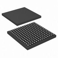
HSP50216KIZ Intersil, HSP50216KIZ Datasheet - Page 46

HSP50216KIZ
Manufacturer Part Number
HSP50216KIZ
Description
IC DOWNCONVERTER DGTL 4CH 196BGA
Manufacturer
Intersil
Datasheet
1.HSP50216KIZ.pdf
(58 pages)
Specifications of HSP50216KIZ
Function
Downconverter
Rf Type
W-CDMA
Package / Case
196-BGA
Lead Free Status / RoHS Status
Lead free / RoHS Compliant
The address decoding for the read source locations is given below. The internal address of the data to be read is written to direct
address 3 (ADD(2:0) = 3) to select and/or fetch the data. A strobe is generated, if needed, to fetch or stabilize the data for reading.
If a strobe is needed, the indirect read address must be written to direct address 3 each time the data is needed. If a strobe is not
needed, the data can be read repeatedly at direct addresses 0 and 1(ADD(2:0) = 0 and 1, respectively) with any changes in the
data showing up immediately. The strobe to sample the AGC gain is generated separately by an indirect write (see IWA *00Fh in
the Tables of Indirect Write Address (IWA) Registers). This allows the AGC gain of all the channels to be sampled
simultaneously.
NOTE: These Indirect Read Addresses are repeated for each channel. In the addresses below, the * field is the channel select nibble. These bits
of the Indirect Address select the target channel register for the data being read. Values of 0 through 3 and F are valid.
*006h
*00Ch
*009h
*00Fh
*100h - *17Fh
*180h - *1FCh
*400h - *43Fh
*440h - *47Fh
*480h - *4FFh
*500h - *5FFh
F806h
P(15:0)
4:0
IRA
The five bits selecting the data type are encoded as follows:
C C D D D,
where CC is the channel number and DDD is the data type.
DDD
000
001
010
011
100
101
110
111
Table of Indirect Read Address (IRA) Registers
I(23:8)
I(7:0),8*zeros
Q(23:8)
Q(7:0),8*zero
Mag(23:8)
Mag(7:0),8*zero
Phase(15:0)
AGC gain (15:0)
TABLE 45. μP FIFO READ ORDER CONTROL REGISTER (GWA = F820h THROUGH F83Fh)
Active Carrier NCO Center Frequency.
Wait Preload, Decr 1&2.
Active Timing NCO Center Freq (Most Significant 32 bits).
AGC gain (must first write to AGC gain read strobe register IWA = *00Fh before reading).
Instruction RAMs.
Instruction RAMs (pointer DRAM).
Coefficient ROM -HBF, const.
Coefficient RAM -1.
Coefficient RAM -2.
Coefficient ROM -Resampler.
Input Level Detector Output.
46
Data Type
TABLE 46. TABLE OF INDIRECT READ ADDRESS (IRA) REGISTERS
The upper 16 bits of the I data path via the FIFO/AGC.
The lower 8 bits of the I data path.
The upper 16 bits of the Q data path via the FIFO/AGC.
The lower 8 bits of the Q data path.
The upper 16 bits of magnitude (after the gain adjust described in channel register)
The lower 8 bits of magnitude.
The upper 16 bits of phase.
The upper 16 bits of the AGC gain.
HSP50216
FUNCTION
FUNCTION
August 17, 2007
FN4557.6


