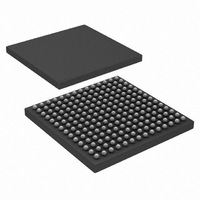
HSP50216KIZ Intersil, HSP50216KIZ Datasheet - Page 32

HSP50216KIZ
Manufacturer Part Number
HSP50216KIZ
Description
IC DOWNCONVERTER DGTL 4CH 196BGA
Manufacturer
Intersil
Datasheet
1.HSP50216KIZ.pdf
(58 pages)
Specifications of HSP50216KIZ
Function
Downconverter
Rf Type
W-CDMA
Package / Case
196-BGA
Lead Free Status / RoHS Status
Lead free / RoHS Compliant
NOTE: These Indirect Write Addresses are repeated for each channel. In the addresses below, the * field is the channel select nibble. These bits
of the Indirect Address select the target channel register for the data. Values of 0 through 3 and F are valid. A channel select nibble value of F is a
special case which writes the data to the same location in each of the four channels simultaneously.
P(15:0)
15:13
8:7
6:4
12
10
11
9
3
Channel Input Source Selection - Selects as the data input for the channel specified in the Indirect Address either A(15:0), B(15:0),
C(15:0), D(15:0) or the μP Test Input register as shown below:
15:13
000
001
010
011
100
μP Test Register input enable selection:
1
0
Select 0 to write test data into the part.
Select 1 to input a constant or to disable the input for minimum power dissipation when an NCO/mixer/CIC section is unused.
μP input enable. When bit 12 is set, this bit is the input enable for the μP Test Register input. Active low:
0
1
Parallel Data Input Format:
0
1
Fixed/Floating point:
0
1
Floating point mantissa size select. The 16-bit data input is grouped as a 13/3 or 14/2 mantissa/exponent word. These control bits
select the mantissa/exponent grouping, add an offset to the exponent and set the shift control saturation level:
00
01
10
11
See the exponent tables contained in the Input Select/Format Block section.
De-multiplex control. These control bits are provided to select a channel from a group of multiplexed channels. Up to 8 multiplexed
data streams can be demultiplexed. These control bits select how many clocks after the ENIx signal to wait before taking the input
sample. ENIx should be asserted for one clock period and aligned with the first channel of the multiplexed data set. For example, if
four streams are multiplexed at half the clock rate, ENIx would align with the first clock period of the first stream, the second would
start two clocks later, the next 4 clocks after ENIx, etc. The samples are aligned with ENIx (zero delay) at the input of the
NCO/Mixer/CIC stage at the next ENIx.
000
111
All values from 0 through 7 are valid.
Interpolated/Gated Mode Select:
0
1
Tables of Indirect Write Address (IWA) Registers
Source Selected
A(15:0)
B(15:0)
C(15:0)
D(15:0)
μP Test input register. This is provided for testing and to zero the input data bus when a channel is not in use. The
Bit 11 of this register is used as the input enable.
A one clock wide pulse generated on each write to lGWA F808h is used as the input enable.
Enabled
Disabled.
Two’s complement (-full scale = 1000...0000, zero = 0000...0000, +full scale = 0111...1111).
Offset binary (-full scale = 0000...0000, zero = 1000...0000, +full scale = 1111...1111).
Fixed point.
Floating point. The 16-bit input bus is divided into mantissa and exponent bits grouped either 13/3 or 14/2 depending on
bits 8 and 7. See text.
11/3: bits 15:5 are mantissa, 2:0 are exponent.
12/3: bits 15:4 are mantissa, 2:0 are exponent.
13/3: bits 15:3 are mantissa, 2:0 are exponent.
14/2: bits 15:2 are mantissa, 1:0 are exponent.
Zero delay
7 clock periods of delay.
Gated. The carrier NCO and CIC are updated once per clock when ENIx is asserted.
Interpolated. The CIC is updated every clock. The carrier NCO is updated once per clock when ENIx is asserted. The
input is zeroed when ENIx is high.
32
TABLE 3. CHANNEL INPUT SELECT/FORMAT REGISTER (IWA = *000h)
Global Write Address register for the μP Test input register is F807h.
HSP50216
FUNCTION
August 17, 2007
FN4557.6


