RMPA2259 Fairchild Semiconductor, RMPA2259 Datasheet
RMPA2259
Specifications of RMPA2259
Available stocks


Related parts for RMPA2259


RMPA2259 Summary of contents
Page 1
... RMPA2259 28dBm WCDMA PowerEdge™ Power Amplifier Module General Description The RMPA2259 power amplifier module (PAM) is designed for WCDMA applications. The 2 stage PAM is internally matched to 50 Ω to minimize the use of external components and features a low power mode to reduce standby current and DC power consumption during peak phone usage ...
Page 2
... No applied RF signal Ratings Units 5.0 V 2.6 to 3.5 V 3.5 V +10 dBm -55 to +150 °C Min Typ Max Units 1920 1980 MHz dBm 16 dBm 450 mA 130 mA -40 dBc -43 dBc -53 dBc -66 dBc 2.0 -139 dBm/Hz -30 dBc -60 dBc 10:1 -30 85 ° µA RMPA2259 Rev. D ...
Page 3
... Low-Power T Case Operating Temperature C Note input power for WCDMA P = +28dBm. OUT ©2004 Fairchild Semiconductor Corporation Parameter Min 1920 3.0 2.7 0 1.8 0 -30 Typ Max Units 1980 MHz 3.4 4.2 V 2.85 3.1 V 0.5 V 2.0 3.0 V 0.5 V +28 dBm +16 dBm +85 °C RMPA2259 Rev. D ...
Page 4
... PAM RMPA2259 W-CDMA 4x4mm Vcc = 3.4V, Vref = 2.85V, Pout = 28dBm -40 -42 -44 -46 -48 -50 -52 -54 -56 -58 -60 1980 2000 1900 1920 2 PAM 1940 1960 1980 2000 FREQUENCY (MHz) Figure 2. 2 PAM 1940 1960 1980 2000 FREQUENCY (MHz) Figure 4. RMPA2259 Rev. D ...
Page 5
... PAM Vref = 2.85V, Pout = 16dBm = 1.2V = 1.5V = 2.0V = 3.0V = 3.4V 1920 1940 1960 1980 FREQUENCY (MHz) Figure 6. 2 PAM Vref = 2.85V, Pout = 16dBm = 1.2V = 1.5V = 2. 3.4V CC 1920 1940 1960 1980 FREQUENCY (MHz) Figure 8. RMPA2259 Rev. D 2000 2000 ...
Page 6
... Vref = 2.85V, Pout = 16dBm, Freq = 1.95GHz 3.5 4 0.5 2 PAM RMPA2259 W-CDMA 4x4mm Vref = 2.85V, Pout = 16dBm, Freq = 1.95GHz -48 -50 -52 -54 -56 -58 -60 -62 -64 -66 -68 3 3.5 4 0.5 2 PAM 1 1.5 2 2.5 3 3.5 V (V) CC Figure 10. 2 PAM 1 1.5 2 2.5 3 3.5 V (V) CC Figure 12. RMPA2259 Rev ...
Page 7
... Vref = 2.85V, Pout = 12dBm, Freq = 1.95GHz 3.5 4 0.5 2 PAM RMPA2259 W-CDMA 4x4mm Vref = 2.85V, Pout = 12dBm, Freq = 1.95GHz -48 -50 -52 -54 -56 -58 -60 -62 -64 -66 -68 3 3.5 4 0.5 2 PAM 1 1.5 2 2.5 3 3.5 V (V) CC Figure 14. 2 PAM 1 1.5 2 2.5 3 3.5 V (V) CC Figure 16. RMPA2259 Rev ...
Page 8
... Vref = 2.85V, Pout = 8dBm, Freq = 1.95GHz 3.5 4 0.5 2 PAM RMPA2259 W-CDMA 4x4mm Vref = 2.85V, Pout = 8dBm, Freq = 1.95GHz -50 -52 -54 -56 -58 -60 -62 -64 -66 -68 -70 3 3.5 4 0.5 2 PAM 1 1.5 2 2.5 3 3.5 V (V) CC Figure 18. 2 PAM 1 1.5 2 2.5 3 3.5 V (V) CC Figure 20. RMPA2259 Rev ...
Page 9
... Rework Considerations: Rework of a device attached to a board is limited to reflow of the solder with a heat gun. The device should not be subjected to more than 225°C and reflow solder in the molten state for more than 5 seconds. No more than 2 rework operations should be performed. RMPA2259 Rev. D ...
Page 10
... Fairchild Semiconductor Corporation SOAK AT 150°C FOR 60 SEC 60 120 TIME (SEC) 1000 pF 1000 RMPA2259 4 PYYWW U31XX 5 11 0.1 µF (PACKAGE BASE) 10 SEC 45 SEC (MAX) 1°C/SEC ABOVE 183°C 180 240 3.3 µF Vcc2 10 SMA2 RF OUT 50 ohm TRL 8 3,6,7,9 RMPA2259 Rev. D 300 ...
Page 11
... SMA Connector Terminals Assembly, RMPA1959 1000pF Capacitor (0603) 1000pF Capacitor (0603) 3.3µF Capacitor (1206) 0.1µF Capacitor (0603) 0.1µF Capacitor (0603) Solder Paste Solder Paste Vendor Fairchild Johnson 3M Fairchild Murata Panasonic TDK Murate Panasonic Indium Corp. Indium Corp RMPA2259 Rev. D ...
Page 12
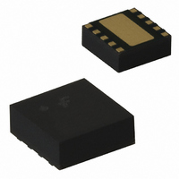
... High-Power/Low-Power Mode Control Vref Reference Voltage GND Ground GND Ground RF Out RF Output Signal GND Ground Vcc2 Supply Voltage to Output Stage GND Paddle Ground 0.1378 (3.50) Typ. 0.1436 (3.65) 0.0069 (0.18) Bottom View Pin 1 Indicator PA2259 PYYWW 7 U31XX 6 Top View RMPA2259 Rev. D ...
Page 13
... TRADEMARKS The following are registered and unregistered trademarks Fairchild Semiconductor owns or is authorized to use and is not intended exhaustive list of all such trademarks. ACEx™ FAST ActiveArray™ FASTr™ Bottomless™ FPS™ CoolFET™ FRFET™ CROSSVOLT™ GlobalOptoisolator™ ...