STEVAL-PCC012V1 STMicroelectronics, STEVAL-PCC012V1 Datasheet - Page 7
STEVAL-PCC012V1
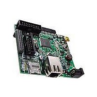
Manufacturer Part Number
STEVAL-PCC012V1
Description
BOARD DEM CONN GATEWAY STM32F107
Manufacturer
STMicroelectronics
Series
STM32r
Type
Other Power Managementr
Datasheets
1.STM32F105V8T6.pdf
(101 pages)
2.STEVAL-PCC012V1.pdf
(10 pages)
3.EVALST7590-1.pdf
(43 pages)
Specifications of STEVAL-PCC012V1
Main Purpose
Interface, Connectivity
Embedded
Yes, MCU, 32-Bit
Utilized Ic / Part
STM32F107
Primary Attributes
Ethernet and 4 Digital/Analog Connectors
Secondary Attributes
On-Board LEDs and Joystick
Interface Type
Ethernet, USB, I2C, SPI, UART
Operating Supply Voltage
3.3 V
Product
Power Management Development Tools
Lead Free Status / RoHS Status
Lead free / RoHS Compliant
For Use With/related Products
STM32F107xx
Other names
497-10757
Available stocks
Company
Part Number
Manufacturer
Quantity
Price
Company:

Part Number:
STEVAL-PCC012V1
Manufacturer:
STMicroelectronics
Quantity:
1


STM32F105xx, STM32F107xx
List of figures
Figure 1.
Figure 2.
Figure 3.
Figure 4.
Figure 5.
Figure 6.
Figure 7.
Figure 8.
Figure 9.
Figure 10.
Figure 11.
Figure 12.
Figure 13.
Figure 14.
Figure 15.
Figure 16.
Figure 17.
Figure 18.
Figure 19.
Figure 20.
Figure 21.
Figure 22.
Figure 23.
Figure 24.
Figure 25.
Figure 26.
Figure 27.
Figure 28.
Figure 29.
Figure 30.
Figure 31.
Figure 32.
Figure 33.
Figure 34.
Figure 35.
Figure 36.
Figure 37.
Figure 38.
Figure 39.
Figure 40.
Figure 41.
Figure 42.
Figure 43.
STM32F105xx and STM32F107xx connectivity line block diagram . . . . . . . . . . . . . . . . . 12
STM32F105xxx and STM32F107xxx connectivity line BGA100 ballout top view. . . . . . . . 23
STM32F105xxx and STM32F107xxx connectivity line LQFP100 pinout . . . . . . . . . . . . . . 24
STM32F105xxx and STM32F107xxx connectivity line LQFP64 pinout . . . . . . . . . . . . . . . 25
Memory map . . . . . . . . . . . . . . . . . . . . . . . . . . . . . . . . . . . . . . . . . . . . . . . . . . . . . . . . . . . . 31
Pin loading conditions . . . . . . . . . . . . . . . . . . . . . . . . . . . . . . . . . . . . . . . . . . . . . . . . . . . . . 32
Pin input voltage . . . . . . . . . . . . . . . . . . . . . . . . . . . . . . . . . . . . . . . . . . . . . . . . . . . . . . . . . 32
Power supply scheme. . . . . . . . . . . . . . . . . . . . . . . . . . . . . . . . . . . . . . . . . . . . . . . . . . . . . 33
Current consumption measurement scheme . . . . . . . . . . . . . . . . . . . . . . . . . . . . . . . . . . . 33
Typical current consumption on V
different V
Typical current consumption in Stop mode with regulator in Run mode
versus temperature at different V
Typical current consumption in Stop mode with regulator in Low-power
mode versus temperature at different V
Typical current consumption in Standby mode versus temperature at
different V
High-speed external clock source AC timing diagram . . . . . . . . . . . . . . . . . . . . . . . . . . . . 46
Low-speed external clock source AC timing diagram . . . . . . . . . . . . . . . . . . . . . . . . . . . . . 46
Typical application with an 8 MHz crystal . . . . . . . . . . . . . . . . . . . . . . . . . . . . . . . . . . . . . . 47
Typical application with a 32.768 kHz crystal . . . . . . . . . . . . . . . . . . . . . . . . . . . . . . . . . . . 48
Standard I/O input characteristics - CMOS port . . . . . . . . . . . . . . . . . . . . . . . . . . . . . . . . . 55
Standard I/O input characteristics - TTL port . . . . . . . . . . . . . . . . . . . . . . . . . . . . . . . . . . . 55
5 V tolerant I/O input characteristics - CMOS port . . . . . . . . . . . . . . . . . . . . . . . . . . . . . . . 56
5 V tolerant I/O input characteristics - TTL port . . . . . . . . . . . . . . . . . . . . . . . . . . . . . . . . . 56
I/O AC characteristics definition . . . . . . . . . . . . . . . . . . . . . . . . . . . . . . . . . . . . . . . . . . . . . 59
Recommended NRST pin protection . . . . . . . . . . . . . . . . . . . . . . . . . . . . . . . . . . . . . . . . . 60
I
SPI timing diagram - slave mode and CPHA = 0 . . . . . . . . . . . . . . . . . . . . . . . . . . . . . . . . 64
SPI timing diagram - slave mode and CPHA = 1
SPI timing diagram - master mode
I
I
USB OTG FS timings: definition of data signal rise and fall time . . . . . . . . . . . . . . . . . . . . 68
Ethernet SMI timing diagram . . . . . . . . . . . . . . . . . . . . . . . . . . . . . . . . . . . . . . . . . . . . . . . 69
Ethernet RMII timing diagram . . . . . . . . . . . . . . . . . . . . . . . . . . . . . . . . . . . . . . . . . . . . . . . 70
Ethernet MII timing diagram . . . . . . . . . . . . . . . . . . . . . . . . . . . . . . . . . . . . . . . . . . . . . . . . 70
ADC accuracy characteristics . . . . . . . . . . . . . . . . . . . . . . . . . . . . . . . . . . . . . . . . . . . . . . . 74
Typical connection diagram using the ADC . . . . . . . . . . . . . . . . . . . . . . . . . . . . . . . . . . . . 74
Power supply and reference decoupling (V
Power supply and reference decoupling (V
12-bit buffered /non-buffered DAC . . . . . . . . . . . . . . . . . . . . . . . . . . . . . . . . . . . . . . . . . . . 77
LFBGA100 - 10 x 10 mm low profile fine pitch ball grid array package
outline . . . . . . . . . . . . . . . . . . . . . . . . . . . . . . . . . . . . . . . . . . . . . . . . . . . . . . . . . . . . . . . . . 80
Recommended PCB design rules (0.80/0.75 mm pitch BGA) . . . . . . . . . . . . . . . . . . . . . . 81
LQFP100, 100-pin low-profile quad flat package outline . . . . . . . . . . . . . . . . . . . . . . . . . . 82
Recommended footprint
LQFP64 – 64 pin low-profile quad flat package outline . . . . . . . . . . . . . . . . . . . . . . . . . . . 83
2
2
2
C bus AC waveforms and measurement circuit . . . . . . . . . . . . . . . . . . . . . . . . . . . . . . . . 62
S slave timing diagram (Philips protocol)
S master timing diagram (Philips protocol)
BAT
DD
values . . . . . . . . . . . . . . . . . . . . . . . . . . . . . . . . . . . . . . . . . . . . . . . . . . . . . . 41
values . . . . . . . . . . . . . . . . . . . . . . . . . . . . . . . . . . . . . . . . . . . . . . . . . . . . . 40
(1)
. . . . . . . . . . . . . . . . . . . . . . . . . . . . . . . . . . . . . . . . . . . . . . . . . 82
Doc ID 15274 Rev 5
DD
BAT
(1)
values . . . . . . . . . . . . . . . . . . . . . . . . . . . . . . . . . . . . 40
. . . . . . . . . . . . . . . . . . . . . . . . . . . . . . . . . . . . . . . . . 65
with RTC on vs. temperature at
DD
(1)
values . . . . . . . . . . . . . . . . . . . . . . . . . . . . . . . 41
REF+
REF+
(1)
. . . . . . . . . . . . . . . . . . . . . . . . . . . . . . . . . . . 67
. . . . . . . . . . . . . . . . . . . . . . . . . . . . . . . . . . 67
(1)
not connected to V
connected to V
. . . . . . . . . . . . . . . . . . . . . . . . . . . . . . 64
DDA
DDA
). . . . . . . . . . . . . . . . . 75
). . . . . . . . . . . . . . 75
List of figures
7/101
Related parts for STEVAL-PCC012V1
Image
Part Number
Description
Manufacturer
Datasheet
Request
R

Part Number:
Description:
Interface Development Tools Opto ISO USB Bridge 8-Pin Motor CTRL BRD
Manufacturer:
STMicroelectronics
Datasheet:

Part Number:
Description:
BOARD EVAL FOR MEMS SENSORS
Manufacturer:
STMicroelectronics
Datasheet:
Part Number:
Description:
EVALBOARD/STEVAL-ISV014V1
Manufacturer:
STMicroelectronics
Part Number:
Description:
BOARD EVAL FOR ST802RT1
Manufacturer:
STMicroelectronics
Datasheet:

Part Number:
Description:
BOARD EVAL FOR VACUUM CLEANER
Manufacturer:
STMicroelectronics
Datasheet:

Part Number:
Description:
KIT DEV STARTER ST10F276Z5
Manufacturer:
STMicroelectronics
Datasheet:

Part Number:
Description:
BOARD LED CTLR/DVR STLED316S
Manufacturer:
STMicroelectronics
Datasheet:

Part Number:
Description:
BOARD EVAL BLDC SENSORLESS MOTOR
Manufacturer:
STMicroelectronics
Datasheet:

Part Number:
Description:
BOARD ELECT FISCAL CASH REGISTER
Manufacturer:
STMicroelectronics
Datasheet:

Part Number:
Description:
BOARD EVAL BIPO SOLUTION FOR PFC
Manufacturer:
STMicroelectronics
Datasheet:
Part Number:
Description:
STMicroelectronics [RIPPLE-CARRY BINARY COUNTER/DIVIDERS]
Manufacturer:
STMicroelectronics
Datasheet:
Part Number:
Description:
STMicroelectronics [LIQUID-CRYSTAL DISPLAY DRIVERS]
Manufacturer:
STMicroelectronics
Datasheet:
Part Number:
Description:
BOARD EVAL FOR MEMS SENSORS
Manufacturer:
STMicroelectronics
Datasheet: