STEVAL-PCC012V1 STMicroelectronics, STEVAL-PCC012V1 Datasheet - Page 30
STEVAL-PCC012V1
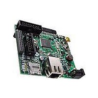
Manufacturer Part Number
STEVAL-PCC012V1
Description
BOARD DEM CONN GATEWAY STM32F107
Manufacturer
STMicroelectronics
Series
STM32r
Type
Other Power Managementr
Datasheets
1.STM32F105V8T6.pdf
(101 pages)
2.STEVAL-PCC012V1.pdf
(10 pages)
3.EVALST7590-1.pdf
(43 pages)
Specifications of STEVAL-PCC012V1
Main Purpose
Interface, Connectivity
Embedded
Yes, MCU, 32-Bit
Utilized Ic / Part
STM32F107
Primary Attributes
Ethernet and 4 Digital/Analog Connectors
Secondary Attributes
On-Board LEDs and Joystick
Interface Type
Ethernet, USB, I2C, SPI, UART
Operating Supply Voltage
3.3 V
Product
Power Management Development Tools
Lead Free Status / RoHS Status
Lead free / RoHS Compliant
For Use With/related Products
STM32F107xx
Other names
497-10757
Available stocks
Company
Part Number
Manufacturer
Quantity
Price
Company:

Part Number:
STEVAL-PCC012V1
Manufacturer:
STMicroelectronics
Quantity:
1


Pinouts and pin description
Table 5.
1. I = input, O = output, S = supply, HiZ = high impedance.
2. FT = 5 V tolerant. All I/Os are V
3. Function availability depends on the chosen device.
4. If several peripherals share the same I/O pin, to avoid conflict between these alternate functions only one peripheral should
5. PC13, PC14 and PC15 are supplied through the power switch, and so their use in output mode is limited: they can be used
6. Main function after the first backup domain power-up. Later on, it depends on the contents of the Backup registers even
7. This alternate function can be remapped by software to some other port pins (if available on the used package). For more
8. SPI2/I2S2 and I2C2 are not available when the Ethernet is being used.
9. For the LQFP64 package, the pins number 5 and 6 are configured as OSC_IN/OSC_OUT after reset, however the
30/101
A7 55 89
A6 56 90
C5 57 91
B5 58 92
A5 59 93
D5 60 94
B4 61 95
A4 62 96
D4
C4
E5 63 99
F5 64 100
be enabled at a time through the peripheral clock enable bit (in the corresponding RCC peripheral clock enable register).
only in output 2 MHz mode with a maximum load of 30 pF and only one pin can be put in output mode at a time.
after reset (because these registers are not reset by the main reset). For details on how to manage these IOs, refer to the
Battery backup domain and BKP register description sections in the STM32F10xxx reference manual, available from the
STMicroelectronics website: www.st.com.
details, refer to the Alternate function I/O and debug configuration section in the STM32F10xxx reference manual,
available from the STMicroelectronics website: www.st.com.
functionality of PD0 and PD1 can be remapped by software on these pins. For the LQFP100 and BGA100 packages, PD0
and PD1 are available by default, so there is no need for remapping. For more details, refer to Alternate function I/O and
debug configuration section in the STM32F10xxx reference manual.
Pins
-
-
97
98
Pin definitions (continued)
Pin name
BOOT0
V
V
PB3
PB4
PB5
PB6
PB7
PB8
PB9
PE0
PE1
DD_3
SS_3
DD
I/O FT
I/O FT
I/O
I/O FT
I/O FT
I/O FT
I/O FT
I/O FT
I/O FT
S
S
I
capable.
(after reset)
function
NJTRST
BOOT0
V
JTDO
V
Main
PB5
PB6
PB7
PB8
PB9
PE0
PE1
DD_3
SS_3
Doc ID 15274 Rev 5
(3)
ETH_MII_PPS_OUT / I2S3_SD
TIM4_CH3
I2C1_SMBA / SPI3_MOSI /
I2C1_SCL
I2C1_SDA
ETH_RMII_PPS_OUT
SPI3_SCK / I2S3_CK
TIM4_CH4
SPI3_MISO
TIM4_ETR
(7)
Default
(7)
(7)
/ ETH_MII_TXD3
/TIM4_CH1
/TIM4_CH2
Alternate functions
(7)
STM32F105xx, STM32F107xx
(7)
(7)
TIM3_CH2/SPI1_MOSI/
USART1_TX/CAN2_TX
TIM2_CH2 / SPI1_SCK
I2C1_SDA / CAN1_TX
I2C1_SCL/CAN1_RX
PB3 / TRACESWO/
PB4 / TIM3_CH1/
(4)
USART1_RX
SPI1_MISO
CAN2_RX
Remap
Related parts for STEVAL-PCC012V1
Image
Part Number
Description
Manufacturer
Datasheet
Request
R

Part Number:
Description:
Interface Development Tools Opto ISO USB Bridge 8-Pin Motor CTRL BRD
Manufacturer:
STMicroelectronics
Datasheet:

Part Number:
Description:
BOARD EVAL FOR MEMS SENSORS
Manufacturer:
STMicroelectronics
Datasheet:
Part Number:
Description:
EVALBOARD/STEVAL-ISV014V1
Manufacturer:
STMicroelectronics
Part Number:
Description:
BOARD EVAL FOR ST802RT1
Manufacturer:
STMicroelectronics
Datasheet:

Part Number:
Description:
BOARD EVAL FOR VACUUM CLEANER
Manufacturer:
STMicroelectronics
Datasheet:

Part Number:
Description:
KIT DEV STARTER ST10F276Z5
Manufacturer:
STMicroelectronics
Datasheet:

Part Number:
Description:
BOARD LED CTLR/DVR STLED316S
Manufacturer:
STMicroelectronics
Datasheet:

Part Number:
Description:
BOARD EVAL BLDC SENSORLESS MOTOR
Manufacturer:
STMicroelectronics
Datasheet:

Part Number:
Description:
BOARD ELECT FISCAL CASH REGISTER
Manufacturer:
STMicroelectronics
Datasheet:

Part Number:
Description:
BOARD EVAL BIPO SOLUTION FOR PFC
Manufacturer:
STMicroelectronics
Datasheet:
Part Number:
Description:
STMicroelectronics [RIPPLE-CARRY BINARY COUNTER/DIVIDERS]
Manufacturer:
STMicroelectronics
Datasheet:
Part Number:
Description:
STMicroelectronics [LIQUID-CRYSTAL DISPLAY DRIVERS]
Manufacturer:
STMicroelectronics
Datasheet:
Part Number:
Description:
BOARD EVAL FOR MEMS SENSORS
Manufacturer:
STMicroelectronics
Datasheet: