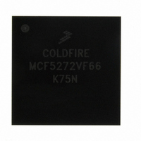
MCF5272VF66 Freescale Semiconductor, MCF5272VF66 Datasheet - Page 452

MCF5272VF66
Manufacturer Part Number
MCF5272VF66
Description
IC MPU 32BIT 66MHZ 196-MAPBGA
Manufacturer
Freescale Semiconductor
Series
MCF527xr
Specifications of MCF5272VF66
Core Processor
Coldfire V2
Core Size
32-Bit
Speed
66MHz
Connectivity
EBI/EMI, Ethernet, I²C, SPI, UART/USART, USB
Peripherals
DMA, WDT
Number Of I /o
32
Program Memory Size
16KB (4K x 32)
Program Memory Type
ROM
Ram Size
1K x 32
Voltage - Supply (vcc/vdd)
3 V ~ 3.6 V
Oscillator Type
External
Operating Temperature
0°C ~ 70°C
Package / Case
196-MAPBGA
Lead Free Status / RoHS Status
Contains lead / RoHS non-compliant
Eeprom Size
-
Data Converters
-
Available stocks
Company
Part Number
Manufacturer
Quantity
Price
Company:
Part Number:
MCF5272VF66
Manufacturer:
HYNIX
Quantity:
19
Company:
Part Number:
MCF5272VF66
Manufacturer:
FREESCAL
Quantity:
885
Company:
Part Number:
MCF5272VF66
Manufacturer:
Freescale Semiconductor
Quantity:
10 000
Part Number:
MCF5272VF66
Manufacturer:
FREESCALE
Quantity:
20 000
Company:
Part Number:
MCF5272VF66J
Manufacturer:
Freescale
Quantity:
256
Company:
Part Number:
MCF5272VF66J
Manufacturer:
Freescale Semiconductor
Quantity:
10 000
Company:
Part Number:
MCF5272VF66R2
Manufacturer:
Freescale Semiconductor
Quantity:
10 000
Company:
Part Number:
MCF5272VF66R2J
Manufacturer:
Freescale Semiconductor
Quantity:
10 000
- Current page: 452 of 544
- Download datasheet (7Mb)
Bus Operation
20.5
The MCF5272 supports byte, word, and longword operands and allows accesses to 8-, 16-, and 32-bit data
ports. The MCF5272 supports port sizes of the specific memory, enables internal generation of transfer
termination, and sets the number of wait states for the external slave being accessed by programming the
CSBRs, CSORs, SDCR, and SDTR. For more information on programming these registers, refer to the
SIM, chip select, and SDRAM controller chapters.
20.5.1
The MCF5272 can be configured for an external physical data bus width of 16 bits by pulling
QSPI_Dout/WSEL high, or for 32 bits by pulling QSPI_Dout/WSEL low during reset. When the external
physical address bus size is configured for 16 bits, the signals D[15:0] become general purpose I/O port C.
The MCF5272 determines the port size for each transfer from the CSBRs at the start of each bus cycle.
This allows the MCF5272 to transfer operands from 8-, 16-, or 32-bit ports. The size of the transfer is
adjusted to accommodate the port size indicated. A 32-bit port must reside on data bus bits D[31:0], a
16-bit port must reside on data bus bits D[31:16], and an 8-bit port must reside on data bus bits D[31:24].
This requirement ensures that the MCF5272 correctly transfers valid data to 8-, 16-, and 32-bit ports.
The bytes of operands are designated as shown in
operand is OP0; OP3 is the least significant byte. The two bytes of a word length operand are OP2 (most
significant) and OP3. The single byte of a byte length operand is OP3. These designations are used in the
figures and descriptions that follow.
20-4
Data Transfer Mechanism
Bus Sizing
The MCF5272 compares the address for the current bus transfer with the
address and mask bits in the CSBRs and CSORs looking for a match. The
priority is listed in
MCF5272 ColdFire
Table 20-2
Table 20-2. Chip Select Memory
®
Priority
Highest
Lowest
Address Decoding Priority
Integrated Microprocessor User’s Manual, Rev. 3
(from highest priority to lowest priority):
NOTE
Figure
Chip Select 0
Chip Select 1
Chip Select 2
Chip Select 3
Chip Select 4
Chip Select 5
Chip Select 6
Chip Select 7
20-1. The most significant byte of a longword
Chip Select
Freescale Semiconductor
Related parts for MCF5272VF66
Image
Part Number
Description
Manufacturer
Datasheet
Request
R
Part Number:
Description:
Mcf5272 Coldfire Integrated Microprocessor User
Manufacturer:
Freescale Semiconductor, Inc
Datasheet:

Part Number:
Description:
MCF5272 Interrupt Service Routine for the Physical Layer Interface Controller
Manufacturer:
Freescale Semiconductor / Motorola
Datasheet:
Part Number:
Description:
Manufacturer:
Freescale Semiconductor, Inc
Datasheet:
Part Number:
Description:
Manufacturer:
Freescale Semiconductor, Inc
Datasheet:
Part Number:
Description:
Manufacturer:
Freescale Semiconductor, Inc
Datasheet:
Part Number:
Description:
Manufacturer:
Freescale Semiconductor, Inc
Datasheet:
Part Number:
Description:
Manufacturer:
Freescale Semiconductor, Inc
Datasheet:
Part Number:
Description:
Manufacturer:
Freescale Semiconductor, Inc
Datasheet:
Part Number:
Description:
Manufacturer:
Freescale Semiconductor, Inc
Datasheet:
Part Number:
Description:
Manufacturer:
Freescale Semiconductor, Inc
Datasheet:
Part Number:
Description:
Manufacturer:
Freescale Semiconductor, Inc
Datasheet:
Part Number:
Description:
Manufacturer:
Freescale Semiconductor, Inc
Datasheet:
Part Number:
Description:
Manufacturer:
Freescale Semiconductor, Inc
Datasheet:
Part Number:
Description:
Manufacturer:
Freescale Semiconductor, Inc
Datasheet:
Part Number:
Description:
Manufacturer:
Freescale Semiconductor, Inc
Datasheet:


