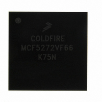
MCF5272VF66 Freescale Semiconductor, MCF5272VF66 Datasheet - Page 431

MCF5272VF66
Manufacturer Part Number
MCF5272VF66
Description
IC MPU 32BIT 66MHZ 196-MAPBGA
Manufacturer
Freescale Semiconductor
Series
MCF527xr
Specifications of MCF5272VF66
Core Processor
Coldfire V2
Core Size
32-Bit
Speed
66MHz
Connectivity
EBI/EMI, Ethernet, I²C, SPI, UART/USART, USB
Peripherals
DMA, WDT
Number Of I /o
32
Program Memory Size
16KB (4K x 32)
Program Memory Type
ROM
Ram Size
1K x 32
Voltage - Supply (vcc/vdd)
3 V ~ 3.6 V
Oscillator Type
External
Operating Temperature
0°C ~ 70°C
Package / Case
196-MAPBGA
Lead Free Status / RoHS Status
Contains lead / RoHS non-compliant
Eeprom Size
-
Data Converters
-
Available stocks
Company
Part Number
Manufacturer
Quantity
Price
Company:
Part Number:
MCF5272VF66
Manufacturer:
HYNIX
Quantity:
19
Company:
Part Number:
MCF5272VF66
Manufacturer:
FREESCAL
Quantity:
885
Company:
Part Number:
MCF5272VF66
Manufacturer:
Freescale Semiconductor
Quantity:
10 000
Part Number:
MCF5272VF66
Manufacturer:
FREESCALE
Quantity:
20 000
Company:
Part Number:
MCF5272VF66J
Manufacturer:
Freescale
Quantity:
256
Company:
Part Number:
MCF5272VF66J
Manufacturer:
Freescale Semiconductor
Quantity:
10 000
Company:
Part Number:
MCF5272VF66R2
Manufacturer:
Freescale Semiconductor
Quantity:
10 000
Company:
Part Number:
MCF5272VF66R2J
Manufacturer:
Freescale Semiconductor
Quantity:
10 000
- Current page: 431 of 544
- Download datasheet (7Mb)
Table 19-6
19.6.3
R/W is programmed on a per-chip-select basis for use with SRAM and external peripheral write accesses.
It should be connected to the external peripheral or memory write enable signal.
R/W acts as a write strobe to external SRAM when the decoded chip select is configured for either of the
two SRAM/ROM modes. It is asserted during on-chip peripherals accesses and negated during on-chip
SRAM accesses.
Freescale Semiconductor
shows how BS[3:0] should be connected to DQMx for 16- and 32-bit SDRAM configurations.
Read/Write (R/W)
In 16-bit bus mode, longword accesses are performed as two sequential
word accesses.
MCF5272 ColdFire
16 Bit 32 Bit
BS3
BS2
NC
NC
5272
BS3
BS2
BS1
BS0
Table 19-6. Connecting BS[3:0] to DQMx
BS1 BS0 Access Size Data Located On
BS3 BS2 Access Type Data Located On
1
1
0
0
1
1
0
0
for 16-Bit Data Bus—SDRAM Cycles
for 16-Bit Data Bus—SRAM Cycles
Table 19-4. Byte Strobe Operation
Table 19-5. Byte Strobe Operation
DQMH
DQML
16 Bit
NC
NC
®
1
0
1
0
1
0
1
0
Integrated Microprocessor User’s Manual, Rev. 3
32 Bit (2 x 16) 32 Bit (1 x 32)
DQMH
DQMH
DQML
DQML
None
Word
None
Word
Byte
Byte
Byte
Byte
NOTE
SDRAM
D[31:24]
D[23:16]
D[31:16]
D[23:16]
D[31:24]
D[31:16]
DQM3
DQM2
DQM1
DQM0
—
—
Data Signals
D[31:24]
D[23:16]
D[15:8]
D[7:0]
Signal Descriptions
19-21
Related parts for MCF5272VF66
Image
Part Number
Description
Manufacturer
Datasheet
Request
R
Part Number:
Description:
Mcf5272 Coldfire Integrated Microprocessor User
Manufacturer:
Freescale Semiconductor, Inc
Datasheet:

Part Number:
Description:
MCF5272 Interrupt Service Routine for the Physical Layer Interface Controller
Manufacturer:
Freescale Semiconductor / Motorola
Datasheet:
Part Number:
Description:
Manufacturer:
Freescale Semiconductor, Inc
Datasheet:
Part Number:
Description:
Manufacturer:
Freescale Semiconductor, Inc
Datasheet:
Part Number:
Description:
Manufacturer:
Freescale Semiconductor, Inc
Datasheet:
Part Number:
Description:
Manufacturer:
Freescale Semiconductor, Inc
Datasheet:
Part Number:
Description:
Manufacturer:
Freescale Semiconductor, Inc
Datasheet:
Part Number:
Description:
Manufacturer:
Freescale Semiconductor, Inc
Datasheet:
Part Number:
Description:
Manufacturer:
Freescale Semiconductor, Inc
Datasheet:
Part Number:
Description:
Manufacturer:
Freescale Semiconductor, Inc
Datasheet:
Part Number:
Description:
Manufacturer:
Freescale Semiconductor, Inc
Datasheet:
Part Number:
Description:
Manufacturer:
Freescale Semiconductor, Inc
Datasheet:
Part Number:
Description:
Manufacturer:
Freescale Semiconductor, Inc
Datasheet:
Part Number:
Description:
Manufacturer:
Freescale Semiconductor, Inc
Datasheet:
Part Number:
Description:
Manufacturer:
Freescale Semiconductor, Inc
Datasheet:


