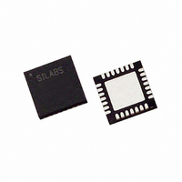
C8051F321 Silicon Laboratories Inc, C8051F321 Datasheet - Page 49

C8051F321
Manufacturer Part Number
C8051F321
Description
IC 8051 MCU 16K FLASH 28MLP
Manufacturer
Silicon Laboratories Inc
Series
C8051F32xr
Datasheet
1.C8051F320R.pdf
(256 pages)
Specifications of C8051F321
Core Processor
8051
Core Size
8-Bit
Speed
25MHz
Connectivity
SMBus (2-Wire/I²C), SPI, UART/USART, USB
Peripherals
Brown-out Detect/Reset, POR, PWM, Temp Sensor, WDT
Number Of I /o
21
Program Memory Size
16KB (16K x 8)
Program Memory Type
FLASH
Ram Size
2.25K x 8
Voltage - Supply (vcc/vdd)
2.7 V ~ 3.6 V
Data Converters
A/D 13x10b
Oscillator Type
Internal
Operating Temperature
-40°C ~ 85°C
Package / Case
28-VQFN Exposed Pad, 28-HVQFN, 28-SQFN, 28-DHVQFN
Lead Free Status / RoHS Status
Contains lead / RoHS non-compliant
Eeprom Size
-
Available stocks
Company
Part Number
Manufacturer
Quantity
Price
Company:
Part Number:
C8051F321
Manufacturer:
SILICON
Quantity:
249
Part Number:
C8051F321
Manufacturer:
SILICON LABS/芯科
Quantity:
20 000
Company:
Part Number:
C8051F321-GM
Manufacturer:
SiliconL
Quantity:
4 364
Part Number:
C8051F321-GM
Manufacturer:
SILICON LABS/芯科
Quantity:
20 000
Part Number:
C8051F321-GMR
Manufacturer:
SILICON LABS/芯科
Quantity:
20 000
Bit7:
Bit6:
Bit5:
Bit4:
Bit3:
Bits2-0:
AD0EN
R/W
Bit7
AD0EN: ADC0 Enable Bit.
0: ADC0 Disabled. ADC0 is in low-power shutdown.
1: ADC0 Enabled. ADC0 is active and ready for data conversions.
AD0TM: ADC0 Track Mode Bit.
0: Normal Track Mode: When ADC0 is enabled, tracking is continuous unless a conversion is in
progress.
1: Low-power Track Mode: Tracking Defined by AD0CM2-0 bits (see below).
AD0INT: ADC0 Conversion Complete Interrupt Flag.
0: ADC0 has not completed a data conversion since the last time AD0INT was cleared.
1: ADC0 has completed a data conversion.
AD0BUSY: ADC0 Busy Bit.
Read:
0: ADC0 conversion is complete or a conversion is not currently in progress. AD0INT is set to
logic 1 on the falling edge of AD0BUSY.
1: ADC0 conversion is in progress.
Write:
0: No Effect.
1: Initiates ADC0 Conversion if AD0CM2-0 = 000b
AD0WINT: ADC0 Window Compare Interrupt Flag.
0: ADC0 Window Comparison Data match has not occurred since this flag was last cleared.
1: ADC0 Window Comparison Data match has occurred.
AD0CM2-0: ADC0 Start of Conversion Mode Select.
When AD0TM = 0:
000: ADC0 conversion initiated on every write of ‘1’ to AD0BUSY.
001: ADC0 conversion initiated on overflow of Timer 0.
010: ADC0 conversion initiated on overflow of Timer 2.
011: ADC0 conversion initiated on overflow of Timer 1.
100: ADC0 conversion initiated on rising edge of external CNVSTR.
101: ADC0 conversion initiated on overflow of Timer 3.
11x: Reserved.
When AD0TM = 1:
000: Tracking initiated on write of ‘1’ to AD0BUSY and lasts 3 SAR clocks, followed by conversion.
001: Tracking initiated on overflow of Timer 0 and lasts 3 SAR clocks, followed by conversion.
010: Tracking initiated on overflow of Timer 2 and lasts 3 SAR clocks, followed by conversion.
011: Tracking initiated on overflow of Timer 1 and lasts 3 SAR clocks, followed by conversion.
100: ADC0 tracks only when CNVSTR input is logic low; conversion starts on rising CNVSTR
edge.
101: Tracking initiated on overflow of Timer 3 and lasts 3 SAR clocks, followed by conversion.
11x: Reserved.
AD0TM
R/W
Bit6
Figure 5.10. ADC0CN: ADC0 Control Register
AD0INT AD0BUSY AD0WINT AD0CM2
R/W
Bit5
R/W
Bit4
R/W
Bit3
Rev. 1.1
R/W
Bit2
AD0CM1
R/W
Bit1
C8051F320/1
(bit addressable)
AD0CM0 00000000
R/W
Bit0
SFR Address:
Reset Value
0xE8
49


