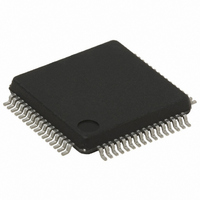
ST7FMC2R7T6TR STMicroelectronics, ST7FMC2R7T6TR Datasheet - Page 32

ST7FMC2R7T6TR
Manufacturer Part Number
ST7FMC2R7T6TR
Description
IC MCU 8BIT 32K FLASH 64-LQFP
Manufacturer
STMicroelectronics
Series
ST7r
Datasheet
1.ST7FMC2S4T6.pdf
(309 pages)
Specifications of ST7FMC2R7T6TR
Core Processor
ST7
Core Size
8-Bit
Speed
8MHz
Connectivity
LINSCI, SPI
Peripherals
LVD, Motor Control PWM, POR, PWM, WDT
Number Of I /o
44
Program Memory Size
48KB (48K x 8)
Program Memory Type
FLASH
Ram Size
1.5K x 8
Voltage - Supply (vcc/vdd)
3.8 V ~ 5.5 V
Data Converters
A/D 16x10b
Oscillator Type
Internal
Operating Temperature
-40°C ~ 85°C
Package / Case
64-LQFP
For Use With
497-8402 - BOARD EVAL COMPLETE INVERTER497-8400 - KIT IGBT PWR MODULE CTRL ST7MC497-6408 - BOARD EVAL BLDC SENSORLESS MOTOR497-4734 - EVAL KIT 3KW POWER DRIVER BOARD497-4733 - EVAL KIT 1KW POWER DRIVER BOARD497-4732 - EVAL KIT 300W POWER DRIVER BOARD497-4731 - EVAL KIT PWR DRIVER CONTROL BRD
Lead Free Status / RoHS Status
Lead free / RoHS Compliant
Eeprom Size
-
Available stocks
Company
Part Number
Manufacturer
Quantity
Price
Company:
Part Number:
ST7FMC2R7T6TR
Manufacturer:
STMicroelectronics
Quantity:
10 000
- Current page: 32 of 309
- Download datasheet (6Mb)
ST7MC1xx/ST7MC2xx
6.3 SYSTEM INTEGRITY MANAGEMENT (SI)
The System Integrity Management block contains
the Low Voltage Detector (LVD), Auxiliary Voltage
Detector (AVD) and Clock Security System (CSS)
functions. It is managed by the SICSR register.
Note: A reset can also be triggered following the
detection of an illegal opcode or prebyte code. Re-
fer to
tails.
6.3.1 Low Voltage Detector (LVD)
The Low Voltage Detector function (LVD) gener-
ates a static reset when the V
below a V
secures the power-up as well as the power-down
keeping the ST7 in reset.
The V
than the V
to avoid a parasitic reset when the MCU starts run-
ning and sinks current on the supply (hysteresis).
The LVD Reset circuitry generates a reset when
V
Figure 17. Low Voltage Detector vs Reset
32/309
1
DD
– V
– V
RESET
is below:
IT-
IT+
IT-
section 11.2.1 on page 244
V
V
reference value for a voltage drop is lower
when V
when V
IT-
IT+
IT+
IT-
reference value for power-on in order
reference value. This means that it
V
DD
DD
DD
is falling
is rising
DD
supply voltage is
for further de-
The LVD function is illustrated in
Provided the minimum V
the oscillator frequency) is above V
can only be in two modes:
In these conditions, secure operation is always en-
sured for the application without the need for ex-
ternal reset hardware.
During a Low Voltage Detector Reset, the RESET
pin is held low, thus permitting the MCU to reset
other devices.
Notes:
The LVD allows the device to be used without any
external RESET circuitry.
The LVD is an optional function which can be se-
lected by option byte.
It is recommended to make sure that the V
ply voltage rises monotonously when the device is
exiting from Reset, to ensure the application func-
tions properly.
V
– under full software control
– in static safe reset
hys
DD
value (guaranteed for
Figure
IT-
, the MCU
17.
DD
sup-
Related parts for ST7FMC2R7T6TR
Image
Part Number
Description
Manufacturer
Datasheet
Request
R

Part Number:
Description:
STMicroelectronics [RIPPLE-CARRY BINARY COUNTER/DIVIDERS]
Manufacturer:
STMicroelectronics
Datasheet:

Part Number:
Description:
STMicroelectronics [LIQUID-CRYSTAL DISPLAY DRIVERS]
Manufacturer:
STMicroelectronics
Datasheet:

Part Number:
Description:
BOARD EVAL FOR MEMS SENSORS
Manufacturer:
STMicroelectronics
Datasheet:

Part Number:
Description:
NPN TRANSISTOR POWER MODULE
Manufacturer:
STMicroelectronics
Datasheet:

Part Number:
Description:
TURBOSWITCH ULTRA-FAST HIGH VOLTAGE DIODE
Manufacturer:
STMicroelectronics
Datasheet:

Part Number:
Description:
Manufacturer:
STMicroelectronics
Datasheet:

Part Number:
Description:
DIODE / SCR MODULE
Manufacturer:
STMicroelectronics
Datasheet:

Part Number:
Description:
DIODE / SCR MODULE
Manufacturer:
STMicroelectronics
Datasheet:

Part Number:
Description:
Search -----> STE16N100
Manufacturer:
STMicroelectronics
Datasheet:

Part Number:
Description:
Search ---> STE53NA50
Manufacturer:
STMicroelectronics
Datasheet:

Part Number:
Description:
NPN Transistor Power Module
Manufacturer:
STMicroelectronics
Datasheet:

Part Number:
Description:
DIODE / SCR MODULE
Manufacturer:
STMicroelectronics
Datasheet:


