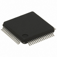
ST7FMC2R7T6TR STMicroelectronics, ST7FMC2R7T6TR Datasheet - Page 267

ST7FMC2R7T6TR
Manufacturer Part Number
ST7FMC2R7T6TR
Description
IC MCU 8BIT 32K FLASH 64-LQFP
Manufacturer
STMicroelectronics
Series
ST7r
Datasheet
1.ST7FMC2S4T6.pdf
(309 pages)
Specifications of ST7FMC2R7T6TR
Core Processor
ST7
Core Size
8-Bit
Speed
8MHz
Connectivity
LINSCI, SPI
Peripherals
LVD, Motor Control PWM, POR, PWM, WDT
Number Of I /o
44
Program Memory Size
48KB (48K x 8)
Program Memory Type
FLASH
Ram Size
1.5K x 8
Voltage - Supply (vcc/vdd)
3.8 V ~ 5.5 V
Data Converters
A/D 16x10b
Oscillator Type
Internal
Operating Temperature
-40°C ~ 85°C
Package / Case
64-LQFP
For Use With
497-8402 - BOARD EVAL COMPLETE INVERTER497-8400 - KIT IGBT PWR MODULE CTRL ST7MC497-6408 - BOARD EVAL BLDC SENSORLESS MOTOR497-4734 - EVAL KIT 3KW POWER DRIVER BOARD497-4733 - EVAL KIT 1KW POWER DRIVER BOARD497-4732 - EVAL KIT 300W POWER DRIVER BOARD497-4731 - EVAL KIT PWR DRIVER CONTROL BRD
Lead Free Status / RoHS Status
Lead free / RoHS Compliant
Eeprom Size
-
Available stocks
Company
Part Number
Manufacturer
Quantity
Price
Company:
Part Number:
ST7FMC2R7T6TR
Manufacturer:
STMicroelectronics
Quantity:
10 000
- Current page: 267 of 309
- Download datasheet (6Mb)
12.9 CONTROL PIN CHARACTERISTICS
12.9.1 Asynchronous RESET Pin
Subject to general operating conditions for V
Notes:
1. Data based on characterization results, not tested in production.
2. Hysteresis voltage between Schmitt trigger switching levels.
3. The I
(I/O ports and control pins) must not exceed I
4. To guarantee the reset of the device, a minimum pulse has to be applied to the RESET pin. All short pulses applied on
RESET pin with a duration below t
5. The reset network protects the device against parasitic resets.
t
w(RSTL)out
t
t
Symbol
h(RSTL)in
g(RSTL)in
R
V
V
V
V
I
hys
IO
ON
OL
IH
IL
IO
current sunk must always respect the absolute maximum rating specified in
Input low level voltage
Input high level voltage
Schmitt trigger voltage hysteresis
Output low level voltage
Driving current on RESET pin
Weak pull-up equivalent resistor
Generated reset pulse duration
External reset pulse hold time
Filtered glitch duration
Parameter
h(RSTL)in
5)
3)
4)
can be ignored.
VSS
2)
.
DD
V
V
Internal reset sources
, f
DD
IN
OSC
=
=5V
V
Conditions
SS,
, and T
V
I
I
DD
IO
IO
=+5mA
=+2mA
=5V
A
unless otherwise specified.
0.7xV
Min
2.5
50
DD
Section 12.2.2
ST7MC1xx/ST7MC2xx
Typ
0.5
0.2
450
80
30
1
2
0.3xV
and the sum of I
Max
150
1.2
0.5
DD
267/309
Unit
mA
kΩ
ns
μs
μs
V
V
V
IO
Related parts for ST7FMC2R7T6TR
Image
Part Number
Description
Manufacturer
Datasheet
Request
R

Part Number:
Description:
STMicroelectronics [RIPPLE-CARRY BINARY COUNTER/DIVIDERS]
Manufacturer:
STMicroelectronics
Datasheet:

Part Number:
Description:
STMicroelectronics [LIQUID-CRYSTAL DISPLAY DRIVERS]
Manufacturer:
STMicroelectronics
Datasheet:

Part Number:
Description:
BOARD EVAL FOR MEMS SENSORS
Manufacturer:
STMicroelectronics
Datasheet:

Part Number:
Description:
NPN TRANSISTOR POWER MODULE
Manufacturer:
STMicroelectronics
Datasheet:

Part Number:
Description:
TURBOSWITCH ULTRA-FAST HIGH VOLTAGE DIODE
Manufacturer:
STMicroelectronics
Datasheet:

Part Number:
Description:
Manufacturer:
STMicroelectronics
Datasheet:

Part Number:
Description:
DIODE / SCR MODULE
Manufacturer:
STMicroelectronics
Datasheet:

Part Number:
Description:
DIODE / SCR MODULE
Manufacturer:
STMicroelectronics
Datasheet:

Part Number:
Description:
Search -----> STE16N100
Manufacturer:
STMicroelectronics
Datasheet:

Part Number:
Description:
Search ---> STE53NA50
Manufacturer:
STMicroelectronics
Datasheet:

Part Number:
Description:
NPN Transistor Power Module
Manufacturer:
STMicroelectronics
Datasheet:

Part Number:
Description:
DIODE / SCR MODULE
Manufacturer:
STMicroelectronics
Datasheet:


