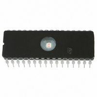
ST7FMC1K2B6 STMicroelectronics, ST7FMC1K2B6 Datasheet - Page 31

ST7FMC1K2B6
Manufacturer Part Number
ST7FMC1K2B6
Description
MCU 8BIT 8K FLASH 32DIP
Manufacturer
STMicroelectronics
Series
ST7r
Datasheet
1.ST7FMC2S4T6.pdf
(309 pages)
Specifications of ST7FMC1K2B6
Core Processor
ST7
Core Size
8-Bit
Speed
8MHz
Connectivity
LINSCI
Peripherals
LVD, Motor Control PWM, POR, PWM, WDT
Number Of I /o
17
Program Memory Size
8KB (8K x 8)
Program Memory Type
FLASH
Ram Size
384 x 8
Voltage - Supply (vcc/vdd)
3.8 V ~ 5.5 V
Data Converters
A/D 16x10b
Oscillator Type
Internal
Operating Temperature
-40°C ~ 85°C
Package / Case
32-DIP (0.600", 15.24mm)
For Use With
497-8402 - BOARD EVAL COMPLETE INVERTER497-8400 - KIT IGBT PWR MODULE CTRL ST7MC497-4734 - EVAL KIT 3KW POWER DRIVER BOARD497-4733 - EVAL KIT 1KW POWER DRIVER BOARD497-4732 - EVAL KIT 300W POWER DRIVER BOARD497-4731 - EVAL KIT PWR DRIVER CONTROL BRD
Lead Free Status / RoHS Status
Lead free / RoHS Compliant
Eeprom Size
-
Other names
497-4864
- Current page: 31 of 309
- Download datasheet (6Mb)
RESET SEQUENCE MANAGER (Cont’d)
The RESET pin is an asynchronous signal which
plays a major role in EMS performance. In a noisy
environment, it is recommended to follow the
guidelines mentioned in the electrical characteris-
tics section.
6.2.3 External Power-On RESET
If the LVD is disabled by option byte, to start up the
microcontroller correctly, the user must ensure by
means of an external reset circuit that the reset
signal is held low until V
level specified for the selected f
A proper reset signal for a slow rising V
can generally be provided by an external RC net-
work connected to the RESET pin.
Figure 16. RESET Sequences
WATCHDOG
RESET
EXTERNAL
RESET
SOURCE
RESET PIN
V
V
IT+(LVD)
IT-(LVD)
V
RUN
DD
ACTIVE PHASE
DD
RESET
LVD
is over the minimum
OSC
frequency.
DD
RUN
t
h(RSTL)in
supply
WATCHDOG UNDERFLOW
ACTIVE
PHASE
EXTERNAL
RESET
6.2.4 Internal Low Voltage Detector (LVD)
RESET
Two different RESET sequences caused by the in-
ternal LVD circuitry can be distinguished:
■
■
The device RESET pin acts as an output that is
pulled low when V
V
The LVD filters spikes on V
avoid parasitic resets.
6.2.5 Internal Watchdog RESET
The RESET sequence generated by a internal
Watchdog counter overflow is shown in
Starting from the Watchdog counter underflow, the
device RESET pin acts as an output that is pulled
low during at least t
DD
Power-On RESET
Voltage Drop RESET
<V
IT-
INTERNAL RESET (256 or 4096 T
VECTOR FETCH
(falling edge) as shown in
RUN
ACTIVE
PHASE
WATCHDOG
RESET
t
w(RSTL)out
w(RSTL)out
DD
ST7MC1xx/ST7MC2xx
<V
DD
IT+
RUN
.
larger than t
CPU
(rising edge) or
)
Figure
Figure
g(VDD)
16.
31/309
16.
to
1
Related parts for ST7FMC1K2B6
Image
Part Number
Description
Manufacturer
Datasheet
Request
R

Part Number:
Description:
STMicroelectronics [RIPPLE-CARRY BINARY COUNTER/DIVIDERS]
Manufacturer:
STMicroelectronics
Datasheet:

Part Number:
Description:
STMicroelectronics [LIQUID-CRYSTAL DISPLAY DRIVERS]
Manufacturer:
STMicroelectronics
Datasheet:

Part Number:
Description:
BOARD EVAL FOR MEMS SENSORS
Manufacturer:
STMicroelectronics
Datasheet:

Part Number:
Description:
NPN TRANSISTOR POWER MODULE
Manufacturer:
STMicroelectronics
Datasheet:

Part Number:
Description:
TURBOSWITCH ULTRA-FAST HIGH VOLTAGE DIODE
Manufacturer:
STMicroelectronics
Datasheet:

Part Number:
Description:
Manufacturer:
STMicroelectronics
Datasheet:

Part Number:
Description:
DIODE / SCR MODULE
Manufacturer:
STMicroelectronics
Datasheet:

Part Number:
Description:
DIODE / SCR MODULE
Manufacturer:
STMicroelectronics
Datasheet:

Part Number:
Description:
Search -----> STE16N100
Manufacturer:
STMicroelectronics
Datasheet:

Part Number:
Description:
Search ---> STE53NA50
Manufacturer:
STMicroelectronics
Datasheet:

Part Number:
Description:
NPN Transistor Power Module
Manufacturer:
STMicroelectronics
Datasheet:

Part Number:
Description:
DIODE / SCR MODULE
Manufacturer:
STMicroelectronics
Datasheet:


