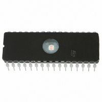
ST7FMC1K2B6 STMicroelectronics, ST7FMC1K2B6 Datasheet - Page 208

ST7FMC1K2B6
Manufacturer Part Number
ST7FMC1K2B6
Description
MCU 8BIT 8K FLASH 32DIP
Manufacturer
STMicroelectronics
Series
ST7r
Datasheet
1.ST7FMC2S4T6.pdf
(309 pages)
Specifications of ST7FMC1K2B6
Core Processor
ST7
Core Size
8-Bit
Speed
8MHz
Connectivity
LINSCI
Peripherals
LVD, Motor Control PWM, POR, PWM, WDT
Number Of I /o
17
Program Memory Size
8KB (8K x 8)
Program Memory Type
FLASH
Ram Size
384 x 8
Voltage - Supply (vcc/vdd)
3.8 V ~ 5.5 V
Data Converters
A/D 16x10b
Oscillator Type
Internal
Operating Temperature
-40°C ~ 85°C
Package / Case
32-DIP (0.600", 15.24mm)
For Use With
497-8402 - BOARD EVAL COMPLETE INVERTER497-8400 - KIT IGBT PWR MODULE CTRL ST7MC497-4734 - EVAL KIT 3KW POWER DRIVER BOARD497-4733 - EVAL KIT 1KW POWER DRIVER BOARD497-4732 - EVAL KIT 300W POWER DRIVER BOARD497-4731 - EVAL KIT PWR DRIVER CONTROL BRD
Lead Free Status / RoHS Status
Lead free / RoHS Compliant
Eeprom Size
-
Other names
497-4864
- Current page: 208 of 309
- Download datasheet (6Mb)
ST7MC1xx/ST7MC2xx
MOTOR CONTROLLER (Cont’d)
A
Read/Write
Reset Value: 0000 0000 (00h)
Bits 7:0 = AN[7:0]: A Weight Value.
These bits contain the A
tiplier. In autoswitched mode the MCOMP register
is automatically loaded with:
when a Z event occurs.
(*) depending on the DCB bit in the MCRA regis-
ter.
PRESCALER & SAMPLING REGISTER
(MPRSR)
Read/Write
Reset Value: 0000 0000 (00h)
Bits 7:4 = SA[3:0]: Sampling Ratio.
These bits contain the sampling ratio value for cur-
rent mode. Refer to Table 47, “Sampling Frequen-
cy Selection,” on page 189.
Bits 3:0 = ST[3:0]: Step Ratio.
These bits contain the step ratio value. It acts as a
prescaler for the MTIM timer and is auto incre-
mented/decremented with each R+ or R- event.
Refer to Table 40, “Step Frequency/Period Range
(4MHz),” on page 179
Accessing MTIM Timer-Related Registers,” on
page 179.
208/309
1
Z
AN7
SA3
N
n
7
7
WEIGHT REGISTER (MWGHT)
x MWGHT
256(d)
AN6
SA2
6
6
AN5
SA1
5
5
or
Z
AN4
SA0
N
4
4
-1
N
x MWGHT
and Table 41, “Modes of
256(d)
weight value for the mul-
AN3
ST3
3
3
AN2
ST2
2
2
(*)
AN1
ST1
1
1
AN0
ST0
0
0
INTERRUPT MASK REGISTER (MIMR)
Read/Write
Reset Value: 0000 0000 (00h)
Bit 7 = PUM: PWM Update Mask bit.
0: PWM Update interrupt disabled
1: PWM Update interrupt enabled
Bit 6 = SEM: Speed Error Mask bit.
0: Speed Error interrupt disabled
1: Speed Error interrupt enabled
Bit 5 = RIM: Ratio update Interrupt Mask bit.
0: Ratio update interrupts (R+ and R-) disabled
1: Ratio update interrupts (R+ and R-) enabled
Bit 4 = CLIM: Current Limitation Interrupt Mask bit.
0: Current Limitation interrupt disabled
1: Current Limitation interrupt enabled
This interrupt is available only in Voltage Mode
(VOC1 bit=0 in MCRA register) and occurs when
the Motor current feedback reaches the external
current limitation value.
Bit 3 = EIM: Emergency stop Interrupt Mask bit.
0: Emergency stop interrupt disabled
1: Emergency stop interrupt enabled
Bit 2 = ZIM: Back EMF Zero-crossing Interrupt
Mask bit.
0: BEMF Zero-crossing Interrupt disabled
1: BEMF Zero-crossing Interrupt enabled
Bit 1 = DIM: End of Demagnetization Interrupt
Mask bit.
0: End of Demagnetization interrupt disabled
1: End of Demagnetization interrupt enabled if the
Bit 0 = CIM: Commutation / Capture Interrupt
Mask bit
0: Commutation / Capture Interrupt disabled
1: Commutation / Capture Interrupt enabled
PUM
HDM or SDM bit in the MCRB register is set
7
SEM
6
RIM
5
CLIM
4
EIM
3
ZIM
2
DIM
1
CIM
0
Related parts for ST7FMC1K2B6
Image
Part Number
Description
Manufacturer
Datasheet
Request
R

Part Number:
Description:
STMicroelectronics [RIPPLE-CARRY BINARY COUNTER/DIVIDERS]
Manufacturer:
STMicroelectronics
Datasheet:

Part Number:
Description:
STMicroelectronics [LIQUID-CRYSTAL DISPLAY DRIVERS]
Manufacturer:
STMicroelectronics
Datasheet:

Part Number:
Description:
BOARD EVAL FOR MEMS SENSORS
Manufacturer:
STMicroelectronics
Datasheet:

Part Number:
Description:
NPN TRANSISTOR POWER MODULE
Manufacturer:
STMicroelectronics
Datasheet:

Part Number:
Description:
TURBOSWITCH ULTRA-FAST HIGH VOLTAGE DIODE
Manufacturer:
STMicroelectronics
Datasheet:

Part Number:
Description:
Manufacturer:
STMicroelectronics
Datasheet:

Part Number:
Description:
DIODE / SCR MODULE
Manufacturer:
STMicroelectronics
Datasheet:

Part Number:
Description:
DIODE / SCR MODULE
Manufacturer:
STMicroelectronics
Datasheet:

Part Number:
Description:
Search -----> STE16N100
Manufacturer:
STMicroelectronics
Datasheet:

Part Number:
Description:
Search ---> STE53NA50
Manufacturer:
STMicroelectronics
Datasheet:

Part Number:
Description:
NPN Transistor Power Module
Manufacturer:
STMicroelectronics
Datasheet:

Part Number:
Description:
DIODE / SCR MODULE
Manufacturer:
STMicroelectronics
Datasheet:


