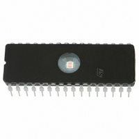
ST7FMC1K2B6 STMicroelectronics, ST7FMC1K2B6 Datasheet - Page 237

ST7FMC1K2B6
Manufacturer Part Number
ST7FMC1K2B6
Description
MCU 8BIT 8K FLASH 32DIP
Manufacturer
STMicroelectronics
Series
ST7r
Datasheet
1.ST7FMC2S4T6.pdf
(309 pages)
Specifications of ST7FMC1K2B6
Core Processor
ST7
Core Size
8-Bit
Speed
8MHz
Connectivity
LINSCI
Peripherals
LVD, Motor Control PWM, POR, PWM, WDT
Number Of I /o
17
Program Memory Size
8KB (8K x 8)
Program Memory Type
FLASH
Ram Size
384 x 8
Voltage - Supply (vcc/vdd)
3.8 V ~ 5.5 V
Data Converters
A/D 16x10b
Oscillator Type
Internal
Operating Temperature
-40°C ~ 85°C
Package / Case
32-DIP (0.600", 15.24mm)
For Use With
497-8402 - BOARD EVAL COMPLETE INVERTER497-8400 - KIT IGBT PWR MODULE CTRL ST7MC497-4734 - EVAL KIT 3KW POWER DRIVER BOARD497-4733 - EVAL KIT 1KW POWER DRIVER BOARD497-4732 - EVAL KIT 300W POWER DRIVER BOARD497-4731 - EVAL KIT PWR DRIVER CONTROL BRD
Lead Free Status / RoHS Status
Lead free / RoHS Compliant
Eeprom Size
-
Other names
497-4864
- Current page: 237 of 309
- Download datasheet (6Mb)
10-BIT A/D CONVERTER (ADC) (Cont’d)
10.8.3.3 Digital A/D Conversion Result
The conversion is monotonic, meaning that the re-
sult never decreases if the analog input does not
and never increases if the analog input does not.
If the input voltage (V
(high-level voltage reference) then the conversion
result is FFh in the ADCDRMSB register and 03h
in the ADCDRLSB register (without overflow indi-
cation).
If the input voltage (V
level voltage reference) then the conversion result
in the ADCDRMSB and ADCDRLSB registers is
00 00h.
The A/D converter is linear and the digital result of
the conversion is stored in the ADCDRMSB and
ADCDRLSB registers. The accuracy of the con-
version is described in the Electrical Characteris-
tics Section.
R
for an analog input signal. If the impedance is too
high, this will result in a loss of accuracy due to
leakage and sampling not being completed in the
alloted time.
R
mented in the device between V
AIN
REF
is the maximum recommended impedance
is the value of the resistive bridge imple-
AIN
AIN
) is lower than V
) is greater than V
REF+
and V
REF-
REF-.
(low-
REF+
10.8.3.4 A/D Conversion
The analog input ports must be configured as in-
put, no pull-up, no interrupt. Refer to the «I/O
ports» chapter. Using these pins as analog inputs
does not affect the ability of the port to be read as
a logic input. If the application used the high-im-
pedance analog inputs, then the sample time
should be stretched by setting the ADSTS bit in
the MCCBCR register.
In the ADCCSR register:
ADC Conversion mode
In the ADCCSR register:
– Set the ADON bit to enable the A/D converter
– The EOC bit is kept low by hardware during the
Note: Changing the A/D channel during conver-
sion will stop the current conversion and start con-
version of the newly selected channel.
and to start the conversion. From this time on,
the ADC performs a continuous conversion of
the selected channel.
conversion.
– Select the CS[3:0] bits to assign the analog
channel to convert.
ST7MC1xx/ST7MC2xx
237/309
Related parts for ST7FMC1K2B6
Image
Part Number
Description
Manufacturer
Datasheet
Request
R

Part Number:
Description:
STMicroelectronics [RIPPLE-CARRY BINARY COUNTER/DIVIDERS]
Manufacturer:
STMicroelectronics
Datasheet:

Part Number:
Description:
STMicroelectronics [LIQUID-CRYSTAL DISPLAY DRIVERS]
Manufacturer:
STMicroelectronics
Datasheet:

Part Number:
Description:
BOARD EVAL FOR MEMS SENSORS
Manufacturer:
STMicroelectronics
Datasheet:

Part Number:
Description:
NPN TRANSISTOR POWER MODULE
Manufacturer:
STMicroelectronics
Datasheet:

Part Number:
Description:
TURBOSWITCH ULTRA-FAST HIGH VOLTAGE DIODE
Manufacturer:
STMicroelectronics
Datasheet:

Part Number:
Description:
Manufacturer:
STMicroelectronics
Datasheet:

Part Number:
Description:
DIODE / SCR MODULE
Manufacturer:
STMicroelectronics
Datasheet:

Part Number:
Description:
DIODE / SCR MODULE
Manufacturer:
STMicroelectronics
Datasheet:

Part Number:
Description:
Search -----> STE16N100
Manufacturer:
STMicroelectronics
Datasheet:

Part Number:
Description:
Search ---> STE53NA50
Manufacturer:
STMicroelectronics
Datasheet:

Part Number:
Description:
NPN Transistor Power Module
Manufacturer:
STMicroelectronics
Datasheet:

Part Number:
Description:
DIODE / SCR MODULE
Manufacturer:
STMicroelectronics
Datasheet:


