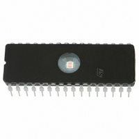
ST7FMC1K2B6 STMicroelectronics, ST7FMC1K2B6 Datasheet - Page 271

ST7FMC1K2B6
Manufacturer Part Number
ST7FMC1K2B6
Description
MCU 8BIT 8K FLASH 32DIP
Manufacturer
STMicroelectronics
Series
ST7r
Datasheet
1.ST7FMC2S4T6.pdf
(309 pages)
Specifications of ST7FMC1K2B6
Core Processor
ST7
Core Size
8-Bit
Speed
8MHz
Connectivity
LINSCI
Peripherals
LVD, Motor Control PWM, POR, PWM, WDT
Number Of I /o
17
Program Memory Size
8KB (8K x 8)
Program Memory Type
FLASH
Ram Size
384 x 8
Voltage - Supply (vcc/vdd)
3.8 V ~ 5.5 V
Data Converters
A/D 16x10b
Oscillator Type
Internal
Operating Temperature
-40°C ~ 85°C
Package / Case
32-DIP (0.600", 15.24mm)
For Use With
497-8402 - BOARD EVAL COMPLETE INVERTER497-8400 - KIT IGBT PWR MODULE CTRL ST7MC497-4734 - EVAL KIT 3KW POWER DRIVER BOARD497-4733 - EVAL KIT 1KW POWER DRIVER BOARD497-4732 - EVAL KIT 300W POWER DRIVER BOARD497-4731 - EVAL KIT PWR DRIVER CONTROL BRD
Lead Free Status / RoHS Status
Lead free / RoHS Compliant
Eeprom Size
-
Other names
497-4864
- Current page: 271 of 309
- Download datasheet (6Mb)
12.11 COMMUNICATION INTERFACE CHARACTERISTICS
12.11.1 SPI - Serial Peripheral Interface
Subject to general operating conditions for V
f
Figure 147. SPI Slave Timing Diagram with CPHA=0
Notes:
1. Data based on design simulation and/or characterisation results, not tested in production.
2. When no communication is on-going the data output line of the SPI (MOSI in master mode, MISO in slave mode) has
its alternate function capability released. In this case, the pin status depends on the I/O port configuration.
3. Measurement points are done at CMOS levels: 0.3xV
4. Depends on f
OSC
Symbol
1/t
t
t
t
t
su(SS)
w(SCKH)
w(SCKL)
t
t
t
h(SS)
t
dis(SO)
t
t
t
t
t
t
r(SCK)
f(SCK)
t
su(MI)
t
h(MO)
f
v(MO)
MISO
MOSI
su(SI)
a(SO)
v(SO)
h(SO)
h(MI)
c(SCK)
h(SI)
, and T
SCK
SS
1)
CPHA=0
CPOL=0
CPHA=0
CPOL=1
1)
OUTPUT
INPUT
INPUT
A
SPI clock frequency
SPI clock rise and fall time
SS setup time
SS hold time
SCK high and low time
Data input setup time
Data input hold time
Data output access time
Data output disable time
Data output valid time
Data output hold time
Data output valid time
Data output hold time
unless otherwise specified.
CPU
see note 2
. For example, if f
t
Parameter
a(SO)
t
su(SS)
t
su(SI)
4)
CPU
t
t
MSB IN
w(SCKH)
w(SCKL)
MSB OUT
=8MHz, then T
t
t
h(SI)
c(SCK)
Master
f
Slave
f
Slave
Slave
Master
Slave
Master
Slave
Master
Slave
Slave
Slave
Slave (after enable edge)
Master (after enable edge)
CPU
CPU
t
DD
v(SO)
=8MHz
=8MHz
DD
CPU
,
BIT6 OUT
Conditions
and 0.7xV
= 1/f
Refer to I/O port characteristics for more details on
the input/output alternate function characteristics
(SS, SCK, MOSI, MISO).
3)
CPU
DD
=125ns and t
BIT1 IN
.
t
h(SO)
(4 x T
su(SS)
f
t
t
CPU
r(SCK)
f(SCK)
0.0625
see I/O port pin description
Min
CPU
120
100
100
100
100
100
90
=550ns
0
0
0
0
/128
ST7MC1xx/ST7MC2xx
) + 50
LSB IN
LSB OUT
t
h(SS)
f
f
CPU
CPU
Max
120
240
120
120
2
4
/4
/2
t
dis(SO)
271/309
Unit
MHz
ns
note 2
see
Related parts for ST7FMC1K2B6
Image
Part Number
Description
Manufacturer
Datasheet
Request
R

Part Number:
Description:
STMicroelectronics [RIPPLE-CARRY BINARY COUNTER/DIVIDERS]
Manufacturer:
STMicroelectronics
Datasheet:

Part Number:
Description:
STMicroelectronics [LIQUID-CRYSTAL DISPLAY DRIVERS]
Manufacturer:
STMicroelectronics
Datasheet:

Part Number:
Description:
BOARD EVAL FOR MEMS SENSORS
Manufacturer:
STMicroelectronics
Datasheet:

Part Number:
Description:
NPN TRANSISTOR POWER MODULE
Manufacturer:
STMicroelectronics
Datasheet:

Part Number:
Description:
TURBOSWITCH ULTRA-FAST HIGH VOLTAGE DIODE
Manufacturer:
STMicroelectronics
Datasheet:

Part Number:
Description:
Manufacturer:
STMicroelectronics
Datasheet:

Part Number:
Description:
DIODE / SCR MODULE
Manufacturer:
STMicroelectronics
Datasheet:

Part Number:
Description:
DIODE / SCR MODULE
Manufacturer:
STMicroelectronics
Datasheet:

Part Number:
Description:
Search -----> STE16N100
Manufacturer:
STMicroelectronics
Datasheet:

Part Number:
Description:
Search ---> STE53NA50
Manufacturer:
STMicroelectronics
Datasheet:

Part Number:
Description:
NPN Transistor Power Module
Manufacturer:
STMicroelectronics
Datasheet:

Part Number:
Description:
DIODE / SCR MODULE
Manufacturer:
STMicroelectronics
Datasheet:


