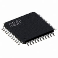
P89CV51RC2FBC,557 NXP Semiconductors, P89CV51RC2FBC,557 Datasheet - Page 63

P89CV51RC2FBC,557
Manufacturer Part Number
P89CV51RC2FBC,557
Description
IC 80C51 MCU FLASH 64K 44-TQFP
Manufacturer
NXP Semiconductors
Series
89Cr
Datasheet
1.P89CV51RB2FA512.pdf
(76 pages)
Specifications of P89CV51RC2FBC,557
Program Memory Type
FLASH
Program Memory Size
32KB (32K x 8)
Package / Case
44-TQFP, 44-VQFP
Core Processor
8051
Core Size
8-Bit
Speed
40MHz
Connectivity
EBI/EMI, SPI, UART/USART
Peripherals
POR, PWM, WDT
Number Of I /o
32
Ram Size
1K x 8
Voltage - Supply (vcc/vdd)
4.5 V ~ 5.5 V
Oscillator Type
Internal
Operating Temperature
-40°C ~ 85°C
Processor Series
P89CV5x
Core
80C51
Data Bus Width
8 bit
Data Ram Size
1 KB
Interface Type
SPI/UART
Maximum Clock Frequency
40 MHz
Number Of Programmable I/os
32
Number Of Timers
3
Operating Supply Voltage
4.5 V to 5.5 V
Maximum Operating Temperature
+ 85 C
Mounting Style
SMD/SMT
3rd Party Development Tools
PK51, CA51, A51, ULINK2
Minimum Operating Temperature
- 40 C
Lead Free Status / RoHS Status
Lead free / RoHS Compliant
Eeprom Size
-
Data Converters
-
Lead Free Status / Rohs Status
Lead free / RoHS Compliant
Other names
568-4255
935284104557
P89CV51RC2FBC
935284104557
P89CV51RC2FBC
Available stocks
Company
Part Number
Manufacturer
Quantity
Price
Company:
Part Number:
P89CV51RC2FBC,557
Manufacturer:
NXP Semiconductors
Quantity:
10 000
NXP Semiconductors
P89CV51RB2_RC2_RD2_3
Product data sheet
Fig 29. External program memory read cycle
PSEN
port 0
port 2
ALE
9.1 Explanation of symbols
Each timing symbol used in
always a ‘t’ (stands for time). The other characters, depending on their positions, stand for
the name of a signal or the logical status of that signal. The following is a list of all the
characters and what they stand for.
A — Address
C — Clock
D — Input data
H — Logic level HIGH
I — Instruction (program memory contents)
L — Logic level LOW or ALE
P — PSEN
Q — Output data
R — RD signal
T — cycle Time
V — Valid
W — WR signal
X — No longer a valid logic level
Z — High impedance (float)
Example:
t
t
AVLL
LLPL
t
= Address valid to ALE LOW time
= ALE LOW to PSEN LOW time
AVLL
t
LHLL
t
LLAX
A0 to A7
t
LLPL
Rev. 03 — 25 August 2009
t AVIV
Figure 29
A8 to A15
t
PLAZ
t
t
to
PLIV
LLIV
INSTR IN
t
P89CV51RB2/RC2/RD2
PXIX
Figure 33
t
PXIZ
t
PLPH
has 5 characters. The first character is
t
PXAV
A0 to A7
A8 to A15
80C51 with 1 kB RAM, SPI
002aaa548
© NXP B.V. 2009. All rights reserved.
63 of 76


