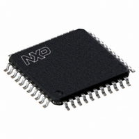
P89CV51RC2FBC,557 NXP Semiconductors, P89CV51RC2FBC,557 Datasheet - Page 6

P89CV51RC2FBC,557
Manufacturer Part Number
P89CV51RC2FBC,557
Description
IC 80C51 MCU FLASH 64K 44-TQFP
Manufacturer
NXP Semiconductors
Series
89Cr
Datasheet
1.P89CV51RB2FA512.pdf
(76 pages)
Specifications of P89CV51RC2FBC,557
Program Memory Type
FLASH
Program Memory Size
32KB (32K x 8)
Package / Case
44-TQFP, 44-VQFP
Core Processor
8051
Core Size
8-Bit
Speed
40MHz
Connectivity
EBI/EMI, SPI, UART/USART
Peripherals
POR, PWM, WDT
Number Of I /o
32
Ram Size
1K x 8
Voltage - Supply (vcc/vdd)
4.5 V ~ 5.5 V
Oscillator Type
Internal
Operating Temperature
-40°C ~ 85°C
Processor Series
P89CV5x
Core
80C51
Data Bus Width
8 bit
Data Ram Size
1 KB
Interface Type
SPI/UART
Maximum Clock Frequency
40 MHz
Number Of Programmable I/os
32
Number Of Timers
3
Operating Supply Voltage
4.5 V to 5.5 V
Maximum Operating Temperature
+ 85 C
Mounting Style
SMD/SMT
3rd Party Development Tools
PK51, CA51, A51, ULINK2
Minimum Operating Temperature
- 40 C
Lead Free Status / RoHS Status
Lead free / RoHS Compliant
Eeprom Size
-
Data Converters
-
Lead Free Status / Rohs Status
Lead free / RoHS Compliant
Other names
568-4255
935284104557
P89CV51RC2FBC
935284104557
P89CV51RC2FBC
Available stocks
Company
Part Number
Manufacturer
Quantity
Price
Company:
Part Number:
P89CV51RC2FBC,557
Manufacturer:
NXP Semiconductors
Quantity:
10 000
NXP Semiconductors
Table 3.
P89CV51RB2_RC2_RD2_3
Product data sheet
Symbol
P0[6]/AD6
P0[7]/AD7
P1[0] to P1[7]
P1[0]/T2
P1[1]/T2EX
P1[2]/ECI
P1[3]/CEX0
P1[4]/CEX1/
SS
P1[5]/CEX2/
MOSI
P1[6]/CEX3/
MISO
P1[7]/CEX4/
SPICLK
P2[0] to P2[7]
P2[0]/A8
P89CV51RB2/RC2/RD2 Pin description
Pin
PLCC44
37
36
2
3
4
5
6
7
8
9
24
TQFP44
31
30
40
41
42
43
44
1
2
3
18
Type
I/O
I/O
I/O
I/O
I/O with
internal
pull-up
I/O
I/O
I/O
I
I/O
I
I/O
I/O
I/O
I/O
I
I/O
I/O
I/O
I/O
I/O
I/O
I/O
I/O
I/O
I/O with
internal
pull-up
I/O
O
Description
P0[6] — Port 0 bit 6.
AD6 — Address/data bit 6.
P0[7] — Port 0 bit 7.
AD7 — Address/data bit 7.
Port 1: Port 1 is an 8-bit bidirectional I/O port with internal pull-ups. The
Port 1 pins are pulled HIGH by the internal pull-ups when 1s are written to
them and can be used as inputs in this state. As inputs, Port 1 pins that are
externally pulled LOW will source current (I
pull-ups. P1[5], P1[6], P1[7] have high current drive of 16 mA.
P1[0] — Port 1 bit 0.
T2 — External count input to timer/counter 2 or clock-out from timer/counter
2.
P1[1] — Port 1 bit 1.
T2EX: Timer/counter 2 capture/reload trigger and direction control.
P1[2] — Port 1 bit 2.
ECI — External clock input. This signal is the external clock input for the
PCA.
P1[3] — Port 1 bit 3.
CEX0 — Capture/compare external I/O for PCA Module 0. Each
capture/compare module connects to a Port 1 pin for external I/O. When not
used by the PCA, this pin can handle standard I/O.
P1[4] — Port 1 bit 4.
CEX1 — Capture/compare external I/O for PCA Module 1.
SS — Slave Select input for SPI.
P1[5] — Port 1 bit 5.
CEX2 — Capture/compare external I/O for PCA Module 2.
MOSI — Master output/slave input for SPI.
P1[6] — Port 1 bit 6.
CEX3 — Capture/compare external I/O for PCA Module 3.
MISO — Master input/slave output for SPI.
P1[7] — Port 1 bit 7.
CEX4 — Capture/compare external I/O for PCA Module 4.
SPICLK — Serial clock input/output for SPI.
Port 2: Port 2 is an 8-bit bidirectional I/O port with internal pull-ups. Port 2
pins are pulled HIGH by the internal pull-ups when 1s are written to them
and can be used as inputs in this state. As inputs, Port 2 pins that are
externally pulled LOW will source current (I
pull-ups. Port 2 sends the high-order address byte during fetches from
external program memory and during accesses to external data memory
that use 16-bit address (MOVX @DPTR). In this application, it uses strong
internal pull-ups when transitioning to 1s.
P2[0] — Port 2 bit 0.
A8 — Address bit 8.
Rev. 03 — 25 August 2009
…continued
P89CV51RB2/RC2/RD2
IL
IL
) because of the internal
) because of the internal
80C51 with 1 kB RAM, SPI
© NXP B.V. 2009. All rights reserved.
6 of 76


