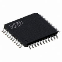
P89CV51RC2FBC,557 NXP Semiconductors, P89CV51RC2FBC,557 Datasheet - Page 14

P89CV51RC2FBC,557
Manufacturer Part Number
P89CV51RC2FBC,557
Description
IC 80C51 MCU FLASH 64K 44-TQFP
Manufacturer
NXP Semiconductors
Series
89Cr
Datasheet
1.P89CV51RB2FA512.pdf
(76 pages)
Specifications of P89CV51RC2FBC,557
Program Memory Type
FLASH
Program Memory Size
32KB (32K x 8)
Package / Case
44-TQFP, 44-VQFP
Core Processor
8051
Core Size
8-Bit
Speed
40MHz
Connectivity
EBI/EMI, SPI, UART/USART
Peripherals
POR, PWM, WDT
Number Of I /o
32
Ram Size
1K x 8
Voltage - Supply (vcc/vdd)
4.5 V ~ 5.5 V
Oscillator Type
Internal
Operating Temperature
-40°C ~ 85°C
Processor Series
P89CV5x
Core
80C51
Data Bus Width
8 bit
Data Ram Size
1 KB
Interface Type
SPI/UART
Maximum Clock Frequency
40 MHz
Number Of Programmable I/os
32
Number Of Timers
3
Operating Supply Voltage
4.5 V to 5.5 V
Maximum Operating Temperature
+ 85 C
Mounting Style
SMD/SMT
3rd Party Development Tools
PK51, CA51, A51, ULINK2
Minimum Operating Temperature
- 40 C
Lead Free Status / RoHS Status
Lead free / RoHS Compliant
Eeprom Size
-
Data Converters
-
Lead Free Status / Rohs Status
Lead free / RoHS Compliant
Other names
568-4255
935284104557
P89CV51RC2FBC
935284104557
P89CV51RC2FBC
Available stocks
Company
Part Number
Manufacturer
Quantity
Price
Company:
Part Number:
P89CV51RC2FBC,557
Manufacturer:
NXP Semiconductors
Quantity:
10 000
NXP Semiconductors
P89CV51RB2_RC2_RD2_3
Product data sheet
The DPTR points to location 0A0H and the data in the accumulator is written to address
0A0H of the expanded RAM rather than off-chip external memory. Access to EXTRAM
addresses that are not present on the device (above 2FFH) will access external off-chip
memory and will perform in the same way as the standard 8051, with P0 and P2 as
data/address bus, and P3[6] and P3[7] as write and read timing signals.
Table 6.
When EXTRAM = 1, MOVX @Ri and MOVX @DPTR will be similar to the standard 8051.
Using MOVX @Ri provides an 8-bit address with multiplexed data on Port 0. Other output
port pins can be used to output higher order address bits. This provides external paging
capabilities. Using MOVX @DPTR generates a 16-bit address. This allows external
addressing up to 64 kB. Port 2 provides the high-order eight address bits (DPH), and
Port 0 multiplexes the low-order eight address bits (DPL) with data. Both MOVX @Ri and
MOVX @DPTR generates the necessary read and write signals (P3[6] - WR and P3[7] -
RD) for external memory use.
with EXTRAM bit.
The stack pointer (SP) can be located anywhere within the 256 B of internal RAM (lower
128 B and upper 128 B). The stack pointer may not be located in any part of the expanded
RAM.
Table 7.
Bit
7 to 2
1
0
AUXR
EXTRAM = 1
EXTRAM = 0
AUXR - Auxiliary function register (address 8EH) bit description
External data memory RD, WR with EXTRAM bit
Symbol
-
EXTRAM
AO
MOVX @DPTR, A or MOVX A, @DPTR
ADDR < 0300H
RD/WR asserted
RD/WR not asserted
Rev. 03 — 25 August 2009
Description
Reserved for future use. Should be set to 0 by user programs.
Internal/external RAM access using MOVX @Ri/@DPTR. When 0,
accesses internal XRAM with address specified in MOVX instruction.
If address supplied with this instruction exceeds on-chip available
XRAM, off-chip RAM is accessed. When 1, every MOVX instruction
targets external data memory by default.
ALE off: disables/enables ALE. AO = 0 results in ALE emitted at a
constant rate of
active only during a MOVX or MOVC.
Table 7
ADDR
RD/WR asserted
RD/WR asserted
shows external data memory RD, WR operation
1
P89CV51RB2/RC2/RD2
2
the oscillator frequency. In case of AO = 1, ALE is
0300H
MOVX @Ri, A or MOVX A, @Ri
ADDR = any
RD/WR asserted
RD/WR not asserted
80C51 with 1 kB RAM, SPI
© NXP B.V. 2009. All rights reserved.
14 of 76


