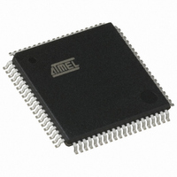
AT80C51SND1C-ROTIL Atmel, AT80C51SND1C-ROTIL Datasheet - Page 75

AT80C51SND1C-ROTIL
Manufacturer Part Number
AT80C51SND1C-ROTIL
Description
IC MCU FLASH MP3 DECODER 80-TQFP
Manufacturer
Atmel
Series
80Cr
Datasheet
1.AT80C51SND1C-ROTIL.pdf
(213 pages)
Specifications of AT80C51SND1C-ROTIL
Core Processor
8051
Core Size
8-Bit
Speed
40MHz
Connectivity
I²C, IDE/ATAPI, MMC, SPI, UART/USART, USB
Peripherals
Audio, I²S, MP3, PCM, POR, WDT
Number Of I /o
44
Program Memory Type
ROMless
Ram Size
2.25K x 8
Voltage - Supply (vcc/vdd)
2.7 V ~ 3.3 V
Data Converters
A/D 2x10b
Oscillator Type
Internal
Operating Temperature
-40°C ~ 85°C
Package / Case
80-TQFP, 80-VQFP
Lead Free Status / RoHS Status
Contains lead / RoHS non-compliant
Eeprom Size
-
Program Memory Size
-
Other names
AT80C51SND1CROTIL
Available stocks
Company
Part Number
Manufacturer
Quantity
Price
- Current page: 75 of 213
- Download datasheet (3Mb)
14.3
4109L–8051–02/08
Data Converter
and its calculation formula. The audio interface clock frequency depends on the incoming MP3
frames and the audio DAC used.
Figure 14-2. Audio Clock Generator and Symbol
As soon as audio interface is enabled by setting AUDEN bit in AUDCON1 register, the master
clock generated by the PLL is output on the SCLK pin which is the DAC system clock. This clock
is output at 256 or 384 times the sampling frequency depending on the DAC capabilities. HLR bit
in AUDCON0 register must be set according to this rate for properly generating the audio bit
clock on the DCLK pin and the word selection clock on the DSEL pin. These clocks are not gen-
erated when no data is available at the data converter input.
For DAC compatibility, the bit clock frequency is programmable for outputting 16 bits or 32 bits
per channel using the DSIZ bit in AUDCON0 register (see Section "Data Converter", page 75),
and the word selection signal is programmable for outputting left channel on low or high level
according to POL bit in AUDCON0 register as shown in Figure 14-3.
Figure 14-3. DSEL Output Polarity
The data converter block converts the audio stream input from the 16-bit parallel format to a
serial format. For accepting all PCM formats and I
are used to shift the data output point. As shown in Figure 14-4, these bits allow MSB justifica-
tion by setting JUST4:0 = 00000, LSB justification by setting JUST4:0 = 10000, I
by setting JUST4:0 = 00001, and more than 16-bit LSB justification by filling the low significant
bits with logic 0.
CLOCK
PLL
POL = 0
POL = 1
AUCD4:0
AUDCLK
Left Channel
Left Channel
AUDclk
Audio Interface Clock
=
2
---------------------------
AUCD
S format, JUST4:0 bits in AUDCON0 register
PLLclk
+
Right Channel
Right Channel
1
AT8xC51SND1C
Audio Clock Symbol
CLOCK
2
AUD
S Justification
75
Related parts for AT80C51SND1C-ROTIL
Image
Part Number
Description
Manufacturer
Datasheet
Request
R

Part Number:
Description:
DEV KIT FOR AVR/AVR32
Manufacturer:
Atmel
Datasheet:

Part Number:
Description:
INTERVAL AND WIPE/WASH WIPER CONTROL IC WITH DELAY
Manufacturer:
ATMEL Corporation
Datasheet:

Part Number:
Description:
Low-Voltage Voice-Switched IC for Hands-Free Operation
Manufacturer:
ATMEL Corporation
Datasheet:

Part Number:
Description:
MONOLITHIC INTEGRATED FEATUREPHONE CIRCUIT
Manufacturer:
ATMEL Corporation
Datasheet:

Part Number:
Description:
AM-FM Receiver IC U4255BM-M
Manufacturer:
ATMEL Corporation
Datasheet:

Part Number:
Description:
Monolithic Integrated Feature Phone Circuit
Manufacturer:
ATMEL Corporation
Datasheet:

Part Number:
Description:
Multistandard Video-IF and Quasi Parallel Sound Processing
Manufacturer:
ATMEL Corporation
Datasheet:

Part Number:
Description:
High-performance EE PLD
Manufacturer:
ATMEL Corporation
Datasheet:

Part Number:
Description:
8-bit Flash Microcontroller
Manufacturer:
ATMEL Corporation
Datasheet:

Part Number:
Description:
2-Wire Serial EEPROM
Manufacturer:
ATMEL Corporation
Datasheet:


