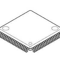
SAB-C161O-LM 3V HA Infineon Technologies, SAB-C161O-LM 3V HA Datasheet - Page 10

SAB-C161O-LM 3V HA
Manufacturer Part Number
SAB-C161O-LM 3V HA
Description
IC MICROCONTROLLER 16BIT MQFP80
Manufacturer
Infineon Technologies
Series
C16xxr
Datasheet
1.SAF-C161O-L25M_HA.pdf
(66 pages)
Specifications of SAB-C161O-LM 3V HA
Core Processor
C166
Core Size
16-Bit
Speed
20MHz
Connectivity
EBI/EMI, SPI, UART/USART
Peripherals
POR, PWM, WDT
Number Of I /o
63
Program Memory Type
ROMless
Ram Size
2K x 8
Voltage - Supply (vcc/vdd)
3 V ~ 3.6 V
Oscillator Type
External
Operating Temperature
0°C ~ 70°C
Package / Case
80-SQFP
Data Bus Width
16 bit
Data Ram Size
2 KB
Interface Type
1xASC, 1xSSC
Maximum Clock Frequency
20 MHz
Number Of Programmable I/os
63
Number Of Timers
5
Operating Supply Voltage
3.3 V
Maximum Operating Temperature
+ 70 C
Mounting Style
SMD/SMT
Minimum Operating Temperature
0 C
Packages
PG-MQFP-80
Max Clock Frequency
20.0 MHz
Sram (incl. Cache)
2.0 KByte
Program Memory
0.0 KByte
Lead Free Status / RoHS Status
Lead free / RoHS Compliant
Eeprom Size
-
Program Memory Size
-
Data Converters
-
Lead Free Status / Rohs Status
Details
Other names
B161OLM3VHAXT
SABC161OLM3VHAXT
SP000011588
SABC161OLM3VHAXT
SP000011588
Table 2
Symbol Pin
RD
WR/
WRL
ALE
EA
PORT0
P0L.0-7
P0H.0-7
PORT1
P1L.0-7
P1H.0-7
Data Sheet
Num
25
26
27
28
29-36
39-46
47-54
55-62
Pin Definitions and Functions (cont’d)
Input
Outp.
O
O
O
I
IO
IO
Function
External Memory Read Strobe. RD is activated for every
external instruction or data read access.
External Memory Write Strobe. In WR-mode this pin is
activated for every external data write access. In WRL-mode
this pin is activated for low byte data write accesses on a 16-
bit bus, and for every data write access on an 8-bit bus. See
WRCFG in register SYSCON for mode selection.
Address Latch Enable Output. Can be used for latching the
address into external memory or an address latch in the
multiplexed bus modes.
External Access Enable pin. A low level at this pin during and
after Reset forces the C161K/O to begin instruction
execution out of external memory. A high level forces
execution out of the internal program memory.
“ROMless” versions must have this pin tied to ‘0’.
PORT0 consists of the two 8-bit bidirectional I/O ports P0L
and P0H. It is bit-wise programmable for input or output via
direction bits. For a pin configured as input, the output driver
is put into high-impedance state. In case of an external bus
configuration, PORT0 serves as the address (A) and
address/data (AD) bus in multiplexed bus modes and as the
data (D) bus in demultiplexed bus modes.
Demultiplexed bus modes:
Data Path Width:
P0L.0 – P0L.7:
P0H.0 – P0H.7:
Multiplexed bus modes:
Data Path Width:
P0L.0 – P0L.7:
P0H.0 – P0H.7:
PORT1 consists of the two 8-bit bidirectional I/O ports P1L
and P1H. It is bit-wise programmable for input or output via
direction bits. For a pin configured as input, the output driver
is put into high-impedance state. PORT1 is used as the 16-
bit address bus (A) in demultiplexed bus modes and also
after switching from a demultiplexed bus mode to a
multiplexed bus mode.
6
8-bit
D0 – D7
I/O
8-bit
AD0 – AD7
A8 – A15
16-bit
D0 – D7
D8 – D15
16-bit
AD0 – AD7
AD8 – AD15
V2.0, 2001-01
C161O
C161K


