SAB-C161O-LM 3V HA Infineon Technologies, SAB-C161O-LM 3V HA Datasheet
SAB-C161O-LM 3V HA
Specifications of SAB-C161O-LM 3V HA
SABC161OLM3VHAXT
SP000011588


Related parts for SAB-C161O-LM 3V HA


SAB-C161O-LM 3V HA Summary of contents
Page 1
...
Page 2
... Infineon Technologies Office. Infineon Technologies Components may only be used in life-support devices or systems with the express written approval of Infineon Technologies failure of such components can reasonably be expected to cause the failure of that life-support device or system affect the safety or effectiveness of that device or system. Life support devices or systems are intended to be implanted in the human body support and/or maintain and sustain and/or protect human life ...
Page 3
...
Page 4
C161K/O Revision History: Previous Version: Page Subjects (major changes since last revision) All Converted to Infineon layout All C161V removed 2 Ordering Codes and Cross-Reference replaced with Derivative Synopsis Open drain functionality described for P2, P3, P6 ...
Page 5
Single-Chip Microcontroller C166 Family C161K/O • High Performance 16-bit CPU with 4-Stage Pipeline – Instruction Cycle Time at 25 MHz CPU Clock – 400 ns Multiplication (16 – Enhanced Boolean Bit Manipulation Facilities – Additional Instructions to ...
Page 6
... SAF-C161K-L25M SAB-C161K-L25M SAF-C161K-LM3V SAB-C161K-LM3V SAF-C161O-LM SAB-C161O-LM SAF-C161O-L25M SAB-C161O-L25M SAF-C161O-LM3V SAB-C161O-LM3V 1) This Data Sheet is valid for devices starting with and including design step HA. For simplicity all versions are referred to by the term C161K/O throughout this document. Ordering Information The ordering code for Infineon microcontrollers provides an exact reference to the required product. This ordering code identifies: • ...
Page 7
Introduction The C161K derivative of the Infineon C166 Family of full featured single-chip CMOS microcontrollers. It combines high CPU performance (up to 12.5 million instructions per second) with peripheral functionality and enhanced IO-capabilities. The C161K/O is especially suited ...
Page 8
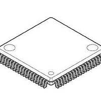
Pin Configuration MQFP Package (top view XTAL1 2 XTAL2 P3.2/CAPIN 5 P3.3/T3OUT 6 P3.4/T3EUD 7 P3.5/T4IN 8 P3.6/T3IN 9 P3.7/T2IN 10 P3.8/MRST 11 P3.9/MTSR 12 P3.10/TxD0 13 P3.11/RxD0 14 P3.12/BHE/WRH 15 P3.13/SCLK 16 ...
Page 9
Table 2 Pin Definitions and Functions Symbol Pin Input Num Outp. XTAL1 2 I XTAL2 P3.8 11 I/O ...
Page 10
Table 2 Pin Definitions and Functions (cont’d) Symbol Pin Input Num Outp WR WRL ALE PORT0 IO P0L.0-7 29-36 P0H.0-7 39-46 PORT1 IO P1L.0-7 47-54 P1H.0-7 55-62 Data Sheet Function ...
Page 11
Table 2 Pin Definitions and Functions (cont’d) Symbol Pin Input Num Outp. RSTIN 65 I/O RST 66 O OUT NMI Data Sheet Function Reset ...
Page 12
Table 2 Pin Definitions and Functions (cont’d) Symbol Pin Input Num Outp P2 P2. P2. P2. P5. P5. ...
Page 13
Functional Description The architecture of the C161K/O combines advantages of both RISC and CISC processors and of advanced peripheral subsystems in a very well-balanced way. In addition the on-chip memory blocks allow the design of compact systems with maximum performance. ...
Page 14
... MBytes. The entire memory space can be accessed bytewise or wordwise. Particular portions of the on-chip memory have additionally been made directly bitaddressable. The C161K/O is prepared to incorporate on-chip program memory (not in the ROM-less derivatives, of course) for code or constant data. The internal ROM area can be mapped either to segment 0 or segment 1 ...
Page 15
External Bus Controller All of the external memory accesses are performed by a particular on-chip External Bus Controller (EBC). It can be programmed either to Single Chip Mode when no external memory is required one of four different ...
Page 16
Central Processing Unit (CPU) The main core of the CPU consists of a 4-stage instruction pipeline, a 16-bit arithmetic and logic unit (ALU) and dedicated SFRs. Additional hardware has been spent for a separate multiply and divide unit, a bit-mask ...
Page 17
The CPU has a register context consisting wordwide GPRs at its disposal. These 16 GPRs are physically allocated within the on-chip RAM area. A Context Pointer (CP) register determines the base address of the active register ...
Page 18
Interrupt System With an interrupt response time within a range from just CPU clocks (in case of internal program execution), the C161K/O is capable of reacting very fast to the occurrence of non-deterministic events. The architecture of ...
Page 19
Table 3 C161K/O Interrupt Nodes Source of Interrupt or PEC Service Request External Interrupt 1 External Interrupt 2 External Interrupt 3 External Interrupt 4 External Interrupt 5 External Interrupt 6 External Interrupt 7 GPT1 Timer 2 GPT1 Timer 3 GPT1 ...
Page 20
The C161K/O also provides an excellent mechanism to identify and to process exceptions or error conditions that arise during run-time, so-called ‘Hardware Traps’. Hardware traps cause immediate non-maskable system reaction which is similar to a standard interrupt service (branching to ...
Page 21
General Purpose Timer (GPT) Unit The GPT unit represents a very flexible multifunctional timer/counter structure which may be used for many different time related tasks such as event timing and counting, pulse width and duty cycle measurements, pulse generation, or ...
Page 22
T2EUD CPU T2IN CPU T3IN T3EUD T4IN CPU T4EUD … 10 Figure 5 Block Diagram of GPT1 With its maximum resolution of ...
Page 23
The capture trigger (timer T5 to CAPREL) may also be generated upon transitions of GPT1 timer T3’s inputs T3IN and/or T3EUD. This is especially advantageous when T3 operates in Incremental Interface Mode. Note: Block GPT2 is only available in the ...
Page 24
Serial Channels Serial communication with other microcontrollers, processors, terminals or external peripheral components is provided by two serial interfaces with different functionality, an Asynchronous/Synchronous Serial Channel (ASC0) and a High-Speed Synchronous Serial Channel (SSC). The ASC0 is upward compatible with ...
Page 25
... Parallel Ports The C161K/O provides I/O lines which are organized into six input/output ports and one input port. All port lines are bit-addressable, and all input/output lines are individually (bit-wise) programmable as inputs or outputs via direction registers. The I/O ports are true bidirectional ports which are switched to high impedance state when configured as inputs ...
Page 26
... BAND, BOR, AND/OR/XOR direct bit with direct bit BXOR BCMP Compare direct bit to direct bit BFLDH/L Bitwise modify masked high/low byte of bit-addressable direct word memory with immediate data CMP(B) Compare word (byte) operands CMPD1/2 Compare word data to GPR and decrement GPR by 1/2 ...
Page 27
... Software Reset IDLE Enter Idle Mode PWRDN Enter Power Down Mode (supposes NMI-pin being low) SRVWDT Service Watchdog Timer DISWDT Disable Watchdog Timer EINIT Signify End-of-Initialization on RSTOUT-pin ATOMIC Begin ATOMIC sequence EXTR Begin EXTended Register sequence EXTP(R) Begin EXTended Page (and Register) sequence ...
Page 28
... The following table lists all SFRs which are implemented in the C161K/O in alphabetical order. Bit-addressable SFRs are marked with the letter “b” in column “Name”. SFRs within the Extended SFR-Space (ESFRs) are marked with the letter “E” in column “Physical Address”. Registers within on-chip X-peripherals are marked with the letter “X” in column “ ...
Page 29
Table 6 C161K/O Registers, Ordered by Name (cont’d) Name Physical Address DP0H b F102 H DP0L b F100 H DP1H b F106 H DP1L b F104 H DP2 b FFC2 H DP3 b FFC6 H DP4 b FFCA H DP6 ...
Page 30
Table 6 C161K/O Registers, Ordered by Name (cont’d) Name Physical Address P3 b FFC4 FFC8 FFA2 FFCC H PECC0 FEC0 H PECC1 FEC2 H PECC2 FEC4 H PECC3 FEC6 H PECC4 ...
Page 31
Table 6 C161K/O Registers, Ordered by Name (cont’d) Name Physical Address SSCEIC b FF76 H SSCRB F0B2 H SSCRIC b FF74 H SSCTB F0B0 H SSCTIC b FF72 H STKOV FE14 H STKUN FE16 H SYSCON b FF12 H T2 ...
Page 32
Absolute Maximum Ratings Table 7 Absolute Maximum Rating Parameters Parameter Storage temperature Junction temperature V Voltage on pins with DD V respect to ground ( ) SS Voltage on any pin with V respect to ground ( ) SS Input ...
Page 33
... > < Unit Notes V Active mode MHz CPUmax V Power Down mode V Active mode MHz CPUmax V Power Down mode V Reference voltage 2)3) mA Per pin – C SAB-C161K/O … C SAF-C161K/O … C SAK-C161K/O … - 0.5 V). The absolute sum of input overload V2.0, 2001-01 C161K C161O ...
Page 34
Parameter Interpretation The parameters listed in the following partly represent the characteristics of the C161K/ O and partly its demands on the system. To aid in interpreting the parameters right, when evaluating them for a design, they are marked in ...
Page 35
DC Characteristics (Standard Supply Voltage Range) (cont’d) (Operating Conditions apply) Parameter 4) RSTIN active current 7) RD/WR inact. current 7) RD/WR active current 7) ALE inactive current 7) ALE active current 7) Port 6 inactive current 7) Port 6 active ...
Page 36
DC Characteristics (Reduced Supply Voltage Range) (Operating Conditions apply) Parameter Input low voltage (TTL, all except XTAL1) Input low voltage XTAL1 Input high voltage (TTL, all except RSTIN and XTAL1) Input high voltage RSTIN (when operated as input) Input high ...
Page 37
DC Characteristics (Reduced Supply Voltage Range) (cont’d) (Operating Conditions apply) Parameter PORT0 configuration current XTAL1 input current 8) Pin capacitance (digital inputs/outputs) 1) Keeping signal levels within the levels specified in this table, ensures operation without overload conditions. For signal ...
Page 38
Power Consumption C161K/O (Standard Supply Voltage Range) (Operating Conditions apply) Parameter Power supply current (active) with all peripherals active Idle mode supply current with all peripherals active Power-down mode supply current 1) The supply current is a function of the ...
Page 39
I mA 100 Figure 7 Supply/Idle Current as a Function of Operating Frequency Data Sheet C161K C161O I DD5max I DD5typ I DD3max I DD3typ I IDX5max I IDX3max I ...
Page 40
AC Characteristics Definition of Internal Timing The internal operation of the C161K/O is controlled by the internal CPU clock edges of the CPU clock can trigger internal (e.g. pipeline) or external (e.g. bus cycles) operations. The specification of the external ...
Page 41
Table 9 C161K/O Clock Generation Modes CLKCFG CPU Frequency f f (P0H.7-5) = CPU OSC OSC OSC 1) The maximum frequency depends on the duty cycle of the external ...
Page 42
AC Characteristics Table 10 External Clock Drive XTAL1 (Standard Supply Voltage Range) (Operating Conditions apply) Parameter Symbol t Oscillator period SR 40 OSC 1) t High time Low time Rise ...
Page 43
V DD Figure 9 External Clock Drive XTAL1 Note: If the on-chip oscillator is used together with a crystal, the oscillator frequency is limited to a range of 4 MHz to 40 MHz strongly recommended to measure ...
Page 44
Testing Waveforms 2 inputs during testing are driven at 2.4 V for a logic 1’ and 0.45 V for a logic 0’. Timing measurements are made at Figure 10 Input Output Waveforms V + 0.1 V ...
Page 45
Memory Cycle Variables The timing tables below use three variables which are derived from the BUSCONx registers and represent the special characteristics of the programmed memory cycle. The following table describes, how these variables are to be computed. Table 12 ...
Page 46
Multiplexed Bus (Standard Supply Voltage Range) (cont’d) (Operating Conditions apply) ALE cycle time = 6 TCL + 2 Parameter RD, WR low time (no RW-delay valid data in (with RW-delay valid data in (no RW-delay) ALE ...
Page 47
Multiplexed Bus (Standard Supply Voltage Range) (cont’d) (Operating Conditions apply) ALE cycle time = 6 TCL + 2 Parameter Address float after RdCS, WrCS (with RW delay) Address float after RdCS, WrCS (no RW delay) RdCS to Valid Data In ...
Page 48
AC Characteristics Multiplexed Bus (Reduced Supply Voltage Range) (Operating Conditions apply) ALE cycle time = 6 TCL + 2 Parameter ALE high time Address setup to ALE Address hold after ALE ALE falling edge to RD, WR (with RW-delay) ALE ...
Page 49
Multiplexed Bus (Reduced Supply Voltage Range) (cont’d) (Operating Conditions apply) ALE cycle time = 6 TCL + 2 Parameter Data float after RD Data valid to WR Data hold after WR ALE rising edge after RD, WR Address hold after ...
Page 50
Multiplexed Bus (Reduced Supply Voltage Range) (cont’d) (Operating Conditions apply) ALE cycle time = 6 TCL + 2 Parameter Data valid to WrCS Data hold after RdCS Data float after RdCS Address hold after RdCS, WrCS Data hold after WrCS ...
Page 51
ALE CSxL A21-A16 (A15-A8) BHE, CSxE Read Cycle BUS RD RdCSx Write Cycle BUS WR, WRL, WRH WrCSx Figure 12 External Memory Cycle: Multiplexed Bus, With Read/Write Delay, Normal ALE Data Sheet ...
Page 52
ALE CSxL A21-A16 (A15-A8) BHE, CSxE t 6 Read Cycle BUS RD RdCSx Write Cycle BUS WR, WRL, WRH WrCSx Figure 13 External Memory Cycle: Multiplexed Bus, With Read/Write Delay, Extended ALE Data Sheet ...
Page 53
ALE CSxL A21-A16 (A15-A8) BHE, CSxE Read Cycle BUS RD RdCSx Write Cycle BUS WR, WRL, WRH WrCSx Figure 14 External Memory Cycle: Multiplexed Bus, No Read/Write Delay, Normal ALE Data Sheet ...
Page 54
ALE CSxL A21-A16 (A15-A8) BHE, CSxE t 6 Read Cycle BUS RD RdCSx Write Cycle BUS WR, WRL, WRH WrCSx Figure 15 External Memory Cycle: Multiplexed Bus, No Read/Write Delay, Extended ALE Data Sheet ...
Page 55
AC Characteristics Demultiplexed Bus (Standard Supply Voltage Range) (Operating Conditions apply) ALE cycle time = 4 TCL + 2 Parameter ALE high time Address setup to ALE ALE falling edge to RD, WR (with RW-delay) ALE falling edge to RD, ...
Page 56
Demultiplexed Bus (Standard Supply Voltage Range) (cont’d) (Operating Conditions apply) ALE cycle time = 4 TCL + 2 Parameter Data valid to WR Data hold after WR ALE rising edge after RD Address hold after WR 3) ALE ...
Page 57
Demultiplexed Bus (Standard Supply Voltage Range) (cont’d) (Operating Conditions apply) ALE cycle time = 4 TCL + 2 Parameter Data float after RdCS 1) (with RW-delay) Data float after RdCS 1) (no RW-delay) Address hold after RdCS, WrCS Data hold ...
Page 58
AC Characteristics Demultiplexed Bus (Reduced Supply Voltage Range) (Operating Conditions apply) ALE cycle time = 4 TCL + 2 Parameter ALE high time Address setup to ALE ALE falling edge to RD, WR (with RW-delay) ALE falling edge to RD, ...
Page 59
Demultiplexed Bus (Reduced Supply Voltage Range) (cont’d) (Operating Conditions apply) ALE cycle time = 4 TCL + 2 Parameter Data valid to WR Data hold after WR ALE rising edge after RD Address hold after WR 3) ALE ...
Page 60
Demultiplexed Bus (Reduced Supply Voltage Range) (cont’d) (Operating Conditions apply) ALE cycle time = 4 TCL + 2 Parameter Data float after RdCS 1) (with RW-delay) Data float after RdCS 1) (no RW-delay) Address hold after RdCS, WrCS Data hold ...
Page 61
ALE CSxL A21-A16 A15-A0 BHE, CSxE Read Cycle BUS (D15-D8) D7-D0 RD RdCSx Write Cycle BUS (D15-D8) D7-D0 WR, WRL, WRH WrCSx Figure 16 External Memory Cycle: Demultiplexed Bus, With Read/Write Delay, Normal ALE Data Sheet ...
Page 62
ALE CSxL A21-A16 A15-A0 BHE, CSxE t 6 Read Cycle BUS (D15-D8) D7-D0 RD RdCSx Write Cycle BUS (D15-D8) D7-D0 WR, WRL, WRH WrCSx Figure 17 External Memory Cycle: Demultiplexed Bus, With Read/Write Delay, Extended ALE Data Sheet ...
Page 63
ALE CSxL A21-A16 A15-A0 BHE, CSxE Read Cycle BUS (D15-D8) D7-D0 RD RdCSx Write Cycle BUS (D15-D8) D7-D0 WR, WRL, WRH WrCSx Figure 18 External Memory Cycle: Demultiplexed Bus, No Read/Write Delay, Normal ALE Data Sheet ...
Page 64
ALE CSxL A21-A16 A15-A0 BHE, CSxE t 6 Read Cycle BUS (D15-D8) D7-D0 RD RdCSx Write Cycle BUS (D15-D8) D7-D0 WR, WRL, WRH WrCSx Figure 19 External Memory Cycle: Demultiplexed Bus, No Read/Write Delay, Extended ALE Data Sheet ...
Page 65
Package Outlines P-MQFP-80-1 (SMD) (Plastic Metric Quad Flat Package) 0.65 0.3 ±0. Index Marking 1) Does not include plastic or metal protrusions of 0.25 max per side Sorts of Packing Package outlines for tubes, trays etc. are ...
Page 66
... Better operating results and business excellence mean less idleness and wastefulness for all of us, more professional success, more accurate information, a better overview and, thereby, less frustration and more satisfaction.” Dr. Ulrich Schumacher Published by Infineon Technologies AG ...