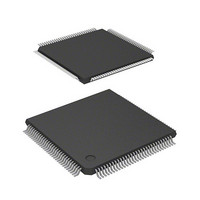
DF2367VTE33 Renesas Electronics America, DF2367VTE33 Datasheet - Page 563

DF2367VTE33
Manufacturer Part Number
DF2367VTE33
Description
IC H8S MCU FLASH 384K 120TQFP
Manufacturer
Renesas Electronics America
Series
H8® H8S/2300r
Specifications of DF2367VTE33
Core Processor
H8S/2000
Core Size
16-Bit
Speed
33MHz
Connectivity
I²C, IrDA, SCI, SmartCard
Peripherals
DMA, POR, PWM, WDT
Number Of I /o
84
Program Memory Size
384KB (384K x 8)
Program Memory Type
FLASH
Ram Size
24K x 8
Voltage - Supply (vcc/vdd)
3 V ~ 3.6 V
Data Converters
A/D 10x10b, D/A 2x8b
Oscillator Type
Internal
Operating Temperature
-20°C ~ 75°C
Package / Case
120-TQFP, 120-VQFP
Lead Free Status / RoHS Status
Contains lead / RoHS non-compliant
Eeprom Size
-
Other names
HD64F2367VTE33
HD64F2367VTE33
HD64F2367VTE33
Available stocks
Company
Part Number
Manufacturer
Quantity
Price
Company:
Part Number:
DF2367VTE33V
Manufacturer:
Renesas Electronics America
Quantity:
10 000
- Current page: 563 of 1044
- Download datasheet (6Mb)
2. Write H'FF in P1DDR and NDERH, and set the G3CMS1, G3CMS0, G2CMS1, and G2CMS0
3. The timer counter in the TPU channel starts. When a compare match with TGRB occurs,
4. Four-phase complementary non-overlapping pulse output can be obtained subsequently by
bits in PCR to select compare match in the TPU channel set up in the previous step to be the
output trigger. Set the G3NOV and G2NOV bits in PMR to 1 to select non-overlapping output.
Write output data H'95 in NDRH.
outputs change from 1 to 0. When a compare match with TGRA occurs, outputs change from 0
to 1 (the change from 0 to 1 is delayed by the value set in TGRA). The TGIA interrupt
handling routine writes the next output data (H'65) in NDRH.
writing H'59, H'56, H'95... at successive TGIA interrupts.
If the DTC or DMAC is set for activation by the TGIA interrupt, pulse output can be obtained
without imposing a load on the CPU.
Section 11 Programmable Pulse Generator (PPG)
Rev.6.00 Mar. 18, 2009 Page 503 of 980
REJ09B0050-0600
Related parts for DF2367VTE33
Image
Part Number
Description
Manufacturer
Datasheet
Request
R

Part Number:
Description:
CONN PLUG 12POS DUAL 0.5MM SMD
Manufacturer:
Hirose Electric Co Ltd
Datasheet:

Part Number:
Description:
CONN PLUG 18POS DUAL 0.5MM SMD
Manufacturer:
Hirose Electric Co Ltd
Datasheet:

Part Number:
Description:
CONN PLUG 14POS DUAL 0.5MM SMD
Manufacturer:
Hirose Electric Co Ltd
Datasheet:

Part Number:
Description:
CONN RECEPT 20POS DUAL 0.5MM SMD
Manufacturer:
Hirose Electric Co Ltd
Datasheet:

Part Number:
Description:
CONN PLUG 16POS DUAL 0.5MM SMD
Manufacturer:
Hirose Electric Co Ltd
Datasheet:

Part Number:
Description:
CONN RECEPT 16POS DUAL 0.5MM SMD
Manufacturer:
Hirose Electric Co Ltd
Datasheet:

Part Number:
Description:
CONN PLUG 20POS DUAL 0.5MM SMD
Manufacturer:
Hirose Electric Co Ltd
Datasheet:

Part Number:
Description:
CONN PLUG 30POS DUAL 0.5MM SMD
Manufacturer:
Hirose Electric Co Ltd
Datasheet:

Part Number:
Description:
CONN RECEPT 30POS DUAL 0.5MM SMD
Manufacturer:
Hirose Electric Co Ltd
Datasheet:

Part Number:
Description:
CONN PLUG 40POS DUAL 0.5MM SMD
Manufacturer:
Hirose Electric Co Ltd
Datasheet:

Part Number:
Description:
KIT STARTER FOR M16C/29
Manufacturer:
Renesas Electronics America
Datasheet:

Part Number:
Description:
KIT STARTER FOR R8C/2D
Manufacturer:
Renesas Electronics America
Datasheet:

Part Number:
Description:
R0K33062P STARTER KIT
Manufacturer:
Renesas Electronics America
Datasheet:

Part Number:
Description:
KIT STARTER FOR R8C/23 E8A
Manufacturer:
Renesas Electronics America
Datasheet:

Part Number:
Description:
KIT STARTER FOR R8C/25
Manufacturer:
Renesas Electronics America
Datasheet:


