DF2367VTE33 Renesas Electronics America, DF2367VTE33 Datasheet - Page 1035
DF2367VTE33
Manufacturer Part Number
DF2367VTE33
Description
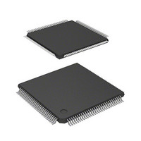
IC H8S MCU FLASH 384K 120TQFP
Manufacturer
Renesas Electronics America
Series
H8® H8S/2300r
Specifications of DF2367VTE33
Core Processor
H8S/2000
Core Size
16-Bit
Speed
33MHz
Connectivity
I²C, IrDA, SCI, SmartCard
Peripherals
DMA, POR, PWM, WDT
Number Of I /o
84
Program Memory Size
384KB (384K x 8)
Program Memory Type
FLASH
Ram Size
24K x 8
Voltage - Supply (vcc/vdd)
3 V ~ 3.6 V
Data Converters
A/D 10x10b, D/A 2x8b
Oscillator Type
Internal
Operating Temperature
-20°C ~ 75°C
Package / Case
120-TQFP, 120-VQFP
Lead Free Status / RoHS Status
Contains lead / RoHS non-compliant
Eeprom Size
-
Other names
HD64F2367VTE33
HD64F2367VTE33
HD64F2367VTE33
Available stocks
Company
Part Number
Manufacturer
Quantity
Price
Company:

Part Number:
DF2367VTE33V
Manufacturer:
Renesas Electronics America
Quantity:
10 000


16-Bit Timer Pulse Unit.......................... 401
8-Bit Timer
8-Bit Timers............................................ 507
A/D Converter ........................................ 661
Address Space........................................... 28
Addressing Mode...................................... 49
Bcc ............................................................ 45
Bus Controller......................................... 119
Buffer Operation................................. 447
Cascaded Operation ............................ 452
Input Capture Function ....................... 444
Phase Counting Mode......................... 459
PWM Modes....................................... 454
Synchronous Operation....................... 445
16-Bit Counter Mode .......................... 520
Compare Match Count Mode ............. 520
Operation with Cascaded Connection. 520
Pulse Output ....................................... 515
TCNT Incrementation Timing ............ 516
A/D Conversion Time......................... 670
A/D Converter Activation................... 468
External Trigger.................................. 673
Scan Mode .......................................... 669
Single Mode........................................ 669
Absolute Address.................................. 50
Immediate ............................................. 51
Memory Indirect ................................... 51
Program-Counter Relative .................... 51
Register Direct ...................................... 49
Register Indirect.................................... 49
Register Indirect with Displacement..... 50
Register Indirect with Post-Increment .. 50
Register indirect with pre-decrement.... 50
Basic Bus Interface ............................. 150
Basic Timing....................................... 153
DRAM Interface ................................. 165
Read Strobe (RD) Timing................... 162
Index
BusController
Clock Pulse Generator ............................ 813
Condition Field .........................................47
Condition-Code Register...........................32
CPU Operating Modes ..............................24
D/A Converter......................................... 681
Data Tranfer Controller
Data Transfer Controller ......................... 293
DMA Controller...................................... 213
Effective Address.......................... 49, 52, 53
Effective Address Extension .....................47
Exception Handling...................................79
Valid Strobes....................................... 152
PLL Circuit ......................................... 818
Advanced Mode ....................................26
Normal Mode ........................................24
Block Transfer Mode .......................... 310
Activation by Software ....................... 316
Chain Transfer .................................... 311
Chain Transfer when Counter = 0....... 318
DTC Vector Table............................... 302
Interrupts ............................................. 312
Location of Register Information........ 302
Normal Mode .............................. 308, 317
Repeat Mode ....................................... 309
Software Activation ............................ 320
Activation by Auto-Request................ 243
Activation by External Request .......... 242
Full Address Mode.............................. 268
Interrupt Sources ................................. 287
Repeat Mode ....................................... 252
Sequential Mode ................................. 246
Short Address Mode............................ 267
Single Address Mode .......................... 256
Transfer Modes ................................... 244
Interrupts ...............................................84
Reset exception handling ......................81
Stack Status after Exception Handling..86
Rev.6.00 Mar. 18, 2009 Page 975 of 980
REJ09B0050-0600
Index
Related parts for DF2367VTE33
Image
Part Number
Description
Manufacturer
Datasheet
Request
R

Part Number:
Description:
CONN PLUG 12POS DUAL 0.5MM SMD
Manufacturer:
Hirose Electric Co Ltd
Datasheet:
Part Number:
Description:
CONN PLUG 18POS DUAL 0.5MM SMD
Manufacturer:
Hirose Electric Co Ltd
Datasheet:
Part Number:
Description:
CONN PLUG 14POS DUAL 0.5MM SMD
Manufacturer:
Hirose Electric Co Ltd
Datasheet:
Part Number:
Description:
CONN RECEPT 20POS DUAL 0.5MM SMD
Manufacturer:
Hirose Electric Co Ltd
Datasheet:
Part Number:
Description:
CONN PLUG 16POS DUAL 0.5MM SMD
Manufacturer:
Hirose Electric Co Ltd
Datasheet:
Part Number:
Description:
CONN RECEPT 16POS DUAL 0.5MM SMD
Manufacturer:
Hirose Electric Co Ltd
Datasheet:
Part Number:
Description:
CONN PLUG 20POS DUAL 0.5MM SMD
Manufacturer:
Hirose Electric Co Ltd
Datasheet:
Part Number:
Description:
CONN PLUG 30POS DUAL 0.5MM SMD
Manufacturer:
Hirose Electric Co Ltd
Datasheet:
Part Number:
Description:
CONN RECEPT 30POS DUAL 0.5MM SMD
Manufacturer:
Hirose Electric Co Ltd
Datasheet:
Part Number:
Description:
CONN PLUG 40POS DUAL 0.5MM SMD
Manufacturer:
Hirose Electric Co Ltd
Datasheet:

Part Number:
Description:
KIT STARTER FOR M16C/29
Manufacturer:
Renesas Electronics America
Datasheet:

Part Number:
Description:
KIT STARTER FOR R8C/2D
Manufacturer:
Renesas Electronics America
Datasheet:

Part Number:
Description:
R0K33062P STARTER KIT
Manufacturer:
Renesas Electronics America
Datasheet:

Part Number:
Description:
KIT STARTER FOR R8C/23 E8A
Manufacturer:
Renesas Electronics America
Datasheet:

Part Number:
Description:
KIT STARTER FOR R8C/25
Manufacturer:
Renesas Electronics America
Datasheet: