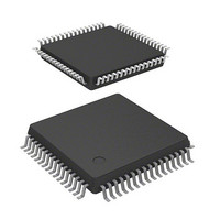
DF36054GFPJV Renesas Electronics America, DF36054GFPJV Datasheet - Page 585

DF36054GFPJV
Manufacturer Part Number
DF36054GFPJV
Description
MCU 3/5V 32K J-TEMP PB-FREE 64-L
Manufacturer
Renesas Electronics America
Series
H8® H8/300H Tinyr
Datasheet
1.DF36057GFZV.pdf
(594 pages)
Specifications of DF36054GFPJV
Core Processor
H8/300H
Core Size
16-Bit
Speed
20MHz
Connectivity
CAN, SCI, SSU
Peripherals
LVD, POR, PWM, WDT
Number Of I /o
45
Program Memory Size
32KB (32K x 8)
Program Memory Type
FLASH
Ram Size
2K x 8
Voltage - Supply (vcc/vdd)
3 V ~ 5.5 V
Data Converters
A/D 8x10b
Oscillator Type
Internal
Operating Temperature
-40°C ~ 85°C
Package / Case
64-LQFP
Lead Free Status / RoHS Status
Lead free / RoHS Compliant
Eeprom Size
-
- Current page: 585 of 594
- Download datasheet (4Mb)
Item
Figure 12.45 Example of Output
Disable Timing of Timer Z by
External Trigger
13.2.1 Timer Control/Status
Register WD (TCSRWD)
16.5 Usage Note
18.3.1 A/D Data Registers A to D
(ADDRA to ADDRD)
Figure 19.1 Block Diagram of
Power-On Reset Circuit and Low-
Voltage Detection Circuit
Page Revision (See Manual for Details)
230
246
378
394
404
Amended
Timer Z
output pin
Amended
Added
Amended
…. The temporary register contents are transferred
from the ADDR when the upper byte data is read.
Therefore, byte access to ADDR should be done by
reading the upper byte first then the lower one. Word
access is also possible. ADDR is initialized to H'0000.
Amended
WKP4
TOER
Bit
4
C
RES
RES
Bit Name
TCSRWE
Timer Z output
N
Rev. 4.00 Mar. 15, 2006 Page 551 of 556
Description
Timer Control/Status Register WD
Write Enable
The WDON and WRST bits can
be written when the TCSRWE bit
is set to 1.
When writing data to this bit, the
value for bit 5 must be 0.
I/O port
REJ09B0026-0400
H'FF
Related parts for DF36054GFPJV
Image
Part Number
Description
Manufacturer
Datasheet
Request
R

Part Number:
Description:
KIT STARTER FOR M16C/29
Manufacturer:
Renesas Electronics America
Datasheet:

Part Number:
Description:
KIT STARTER FOR R8C/2D
Manufacturer:
Renesas Electronics America
Datasheet:

Part Number:
Description:
R0K33062P STARTER KIT
Manufacturer:
Renesas Electronics America
Datasheet:

Part Number:
Description:
KIT STARTER FOR R8C/23 E8A
Manufacturer:
Renesas Electronics America
Datasheet:

Part Number:
Description:
KIT STARTER FOR R8C/25
Manufacturer:
Renesas Electronics America
Datasheet:

Part Number:
Description:
KIT STARTER H8S2456 SHARPE DSPLY
Manufacturer:
Renesas Electronics America
Datasheet:

Part Number:
Description:
KIT STARTER FOR R8C38C
Manufacturer:
Renesas Electronics America
Datasheet:

Part Number:
Description:
KIT STARTER FOR R8C35C
Manufacturer:
Renesas Electronics America
Datasheet:

Part Number:
Description:
KIT STARTER FOR R8CL3AC+LCD APPS
Manufacturer:
Renesas Electronics America
Datasheet:

Part Number:
Description:
KIT STARTER FOR RX610
Manufacturer:
Renesas Electronics America
Datasheet:

Part Number:
Description:
KIT STARTER FOR R32C/118
Manufacturer:
Renesas Electronics America
Datasheet:

Part Number:
Description:
KIT DEV RSK-R8C/26-29
Manufacturer:
Renesas Electronics America
Datasheet:

Part Number:
Description:
KIT STARTER FOR SH7124
Manufacturer:
Renesas Electronics America
Datasheet:

Part Number:
Description:
KIT STARTER FOR H8SX/1622
Manufacturer:
Renesas Electronics America
Datasheet:

Part Number:
Description:
KIT DEV FOR SH7203
Manufacturer:
Renesas Electronics America
Datasheet:


