M30263F6AFP#U5A Renesas Electronics America, M30263F6AFP#U5A Datasheet - Page 350
M30263F6AFP#U5A
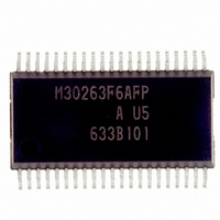
Manufacturer Part Number
M30263F6AFP#U5A
Description
IC M16C/26A MCU FLASH 42-SSOP
Manufacturer
Renesas Electronics America
Series
M16C™ M16C/Tiny/26r
Datasheet
1.M30260F3AGPU5A.pdf
(354 pages)
Specifications of M30263F6AFP#U5A
Core Processor
M16C/60
Core Size
16-Bit
Speed
20MHz
Connectivity
I²C, IEBus, SIO, UART/USART
Peripherals
DMA, PWM, Voltage Detect, WDT
Number Of I /o
33
Program Memory Size
48KB (48K x 8)
Program Memory Type
FLASH
Ram Size
2K x 8
Voltage - Supply (vcc/vdd)
2.7 V ~ 5.5 V
Data Converters
A/D 10x10b
Oscillator Type
Internal
Operating Temperature
-20°C ~ 85°C
Package / Case
42-SSOP
For Use With
R0K33026AS000BE - KIT DEV EVALUATION M16C/26A
Lead Free Status / RoHS Status
Lead free / RoHS Compliant
Eeprom Size
-


Rev.
REVISION HISTORY
Date
Page
108
115
121
123
131
133
136
138
139
142
145
150
154
158
168
175
177
180
183
205
212
77
78
80
81
-
M16C/26A Group (M16C/26A, M16C/26B, M16C/26T) Hardware Manual
•9.7 NMI Interrupt Description partially added
•Table 9.9.1 Value of the PC that is saved to the stack area when an address
Watchdog Timer
•Section of Cold Start/Warm Start deleted
•Description partially added
•Figure 10.1 Watchdog Timer Block Diagram partially modified
•Figure 10.2 WDC Register and WDTS Register notes deleted, WDC5 bit de-
•10.1 Count source protective mode description partially added
Timer
•Description about A/D trigger mode modified
•Figure 12.2.1 Timber B Block Diagram A/D trigger mode added
•12.2.4 A/D Trigger Mode Description modified
•Figure 12.3.4 IDB0 Register, IDB1 Register, DTT Register, and ICTB2 Regis-
•Figure 12.3.6 TB2SC Register modified, note 4 added
•Figure 12.3.2.2 TPRC Register bit map modified
Serial I/O
•Figure 13.1.1 Block Diagram of UARTi (i = 0 to 2) PLL clock added
•Figure 13.1.4 U0TB to U2TB Registers, U0RB to U2RB Registers, U0BRG to
•Figure 13.1.6 U0C0 to U2C0 Registers Note 2 modified, note 7 added
•Figure 13.1.7 PACR Register note 1 modified
•Table 13.1.1.1 Clock Synchronous Serial I/O Mode Specification note 2 modi-
•Figure 13.1.1.1 Typical Transmit/Receive Timings in Clock Synchronous
•Table 13.1.2.1 UART Mode Specifications Note 1 modified
•Figure 13.1.2.2 Receive Operation Figure modified
•Table 13.1.3.1 I
•Table 13.1.4.1 Special Mode 2 Specifications note 2 modified
•Table 13.1.6.1 SIM Mode Specifications note 1 modified
•Figure 13.1.6.1 Transmit and Receive Timing in SIM Mode timing modified
A/D Converter
•Table 14.1 A/D Converter Performance note 2 partially added
•Table 14.2 A/D Conversion Frequency Select note 1 partially added
•Table 14.1.8.1 Delayed Trigger Mode 1 Specifications note 1 modified
•Figure 14.5.1 Analog Input Pin and External Sensor Equivalent Circuit note
match interrupt request is accepted modified, note 1 added
leted
ter modified
U2BRG Registers modified, note 3 for UiBRG added
fied
Serial I/O Mode partially modified
______
2
C bus Mode Specifications note 2 modified
C-2
Description
Summary
Related parts for M30263F6AFP#U5A
Image
Part Number
Description
Manufacturer
Datasheet
Request
R

Part Number:
Description:
KIT STARTER FOR M16C/29
Manufacturer:
Renesas Electronics America
Datasheet:

Part Number:
Description:
KIT STARTER FOR R8C/2D
Manufacturer:
Renesas Electronics America
Datasheet:

Part Number:
Description:
R0K33062P STARTER KIT
Manufacturer:
Renesas Electronics America
Datasheet:

Part Number:
Description:
KIT STARTER FOR R8C/23 E8A
Manufacturer:
Renesas Electronics America
Datasheet:

Part Number:
Description:
KIT STARTER FOR R8C/25
Manufacturer:
Renesas Electronics America
Datasheet:

Part Number:
Description:
KIT STARTER H8S2456 SHARPE DSPLY
Manufacturer:
Renesas Electronics America
Datasheet:

Part Number:
Description:
KIT STARTER FOR R8C38C
Manufacturer:
Renesas Electronics America
Datasheet:

Part Number:
Description:
KIT STARTER FOR R8C35C
Manufacturer:
Renesas Electronics America
Datasheet:

Part Number:
Description:
KIT STARTER FOR R8CL3AC+LCD APPS
Manufacturer:
Renesas Electronics America
Datasheet:
Part Number:
Description:
KIT STARTER FOR RX610
Manufacturer:
Renesas Electronics America
Datasheet:

Part Number:
Description:
KIT STARTER FOR R32C/118
Manufacturer:
Renesas Electronics America
Datasheet:

Part Number:
Description:
KIT DEV RSK-R8C/26-29
Manufacturer:
Renesas Electronics America
Datasheet:

Part Number:
Description:
KIT STARTER FOR SH7124
Manufacturer:
Renesas Electronics America
Datasheet:

Part Number:
Description:
KIT STARTER FOR H8SX/1622
Manufacturer:
Renesas Electronics America
Datasheet:

Part Number:
Description:
KIT DEV FOR SH7203
Manufacturer:
Renesas Electronics America
Datasheet: