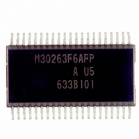
M30263F6AFP#U5A Renesas Electronics America, M30263F6AFP#U5A Datasheet - Page 197

M30263F6AFP#U5A
Manufacturer Part Number
M30263F6AFP#U5A
Description
IC M16C/26A MCU FLASH 42-SSOP
Manufacturer
Renesas Electronics America
Series
M16C™ M16C/Tiny/26r
Datasheet
1.M30260F3AGPU5A.pdf
(354 pages)
Specifications of M30263F6AFP#U5A
Core Processor
M16C/60
Core Size
16-Bit
Speed
20MHz
Connectivity
I²C, IEBus, SIO, UART/USART
Peripherals
DMA, PWM, Voltage Detect, WDT
Number Of I /o
33
Program Memory Size
48KB (48K x 8)
Program Memory Type
FLASH
Ram Size
2K x 8
Voltage - Supply (vcc/vdd)
2.7 V ~ 5.5 V
Data Converters
A/D 10x10b
Oscillator Type
Internal
Operating Temperature
-20°C ~ 85°C
Package / Case
42-SSOP
For Use With
R0K33026AS000BE - KIT DEV EVALUATION M16C/26A
Lead Free Status / RoHS Status
Lead free / RoHS Compliant
Eeprom Size
-
- Current page: 197 of 354
- Download datasheet (4Mb)
R
R
M
e
E
1
. v
J
Figure 13.1.6.2. SIM Interface Connection
Figure 13.1.6.1.1. Parity Error Signal Output Timing
6
0
2
C
9
0 .
B
Figure 13.1.6.2 shows the example of connecting the SIM interface. Connect T
pull-up.
2 /
0
0
13.1.6.1 Parity Error Signal Output
6
U2C1 register
This timing diagram applies to the case where the direct format is implemented.
2
NOTE:
The parity error signal is enabled by setting the U2ERE bit in the U2C1 register’ to “1”.
• When receiving
The parity error signal is output when a parity error is detected while receiving data. This is achieved
by pulling the TxD2 output low with the timing shown in Figure 13.1.6.1.1. If the R2RB register is read
while outputting a parity error signal, the PER bit is cleared to “0” and at the same time the TxD2 output
is returned high.
• When transmitting
A transmission-finished interrupt request is generated at the falling edge of the transfer clock pulse
that immediately follows the stop bit. Therefore, whether a parity signal has been returned can be
determined by reading the port that shares the RxD2 pin in a transmission-finished interrupt service
routine.
A
0
F
2
e
1. The output of microcomputer is in the high-impedance state
G
0 -
b
1 .
o r
Transfer
2
(pulled up externally).
0
, 5
u
0
RxD
RI bit
TxD
p
clock
2
0
(
M
0
2
2
7
1
6
C
page 178
“H”
“L”
“H”
“L”
“H”
“L”
“1”
“0”
2 /
6
, A
M
1
f o
ST
Microcomputer
6
3
C
2
2 /
9
D0
6
, B
RxD
TxD
D1
M
1
2
2
6
C
D2
2 /
6
) T
D3
(1)
D4
D5
D6
SIM card
D7
P
SP
X
D
ST: Start bit
P: Even Parity
SP: Stop bit
2
and R
X
D
2
13. Serial I/O
and apply
Related parts for M30263F6AFP#U5A
Image
Part Number
Description
Manufacturer
Datasheet
Request
R

Part Number:
Description:
KIT STARTER FOR M16C/29
Manufacturer:
Renesas Electronics America
Datasheet:

Part Number:
Description:
KIT STARTER FOR R8C/2D
Manufacturer:
Renesas Electronics America
Datasheet:

Part Number:
Description:
R0K33062P STARTER KIT
Manufacturer:
Renesas Electronics America
Datasheet:

Part Number:
Description:
KIT STARTER FOR R8C/23 E8A
Manufacturer:
Renesas Electronics America
Datasheet:

Part Number:
Description:
KIT STARTER FOR R8C/25
Manufacturer:
Renesas Electronics America
Datasheet:

Part Number:
Description:
KIT STARTER H8S2456 SHARPE DSPLY
Manufacturer:
Renesas Electronics America
Datasheet:

Part Number:
Description:
KIT STARTER FOR R8C38C
Manufacturer:
Renesas Electronics America
Datasheet:

Part Number:
Description:
KIT STARTER FOR R8C35C
Manufacturer:
Renesas Electronics America
Datasheet:

Part Number:
Description:
KIT STARTER FOR R8CL3AC+LCD APPS
Manufacturer:
Renesas Electronics America
Datasheet:

Part Number:
Description:
KIT STARTER FOR RX610
Manufacturer:
Renesas Electronics America
Datasheet:

Part Number:
Description:
KIT STARTER FOR R32C/118
Manufacturer:
Renesas Electronics America
Datasheet:

Part Number:
Description:
KIT DEV RSK-R8C/26-29
Manufacturer:
Renesas Electronics America
Datasheet:

Part Number:
Description:
KIT STARTER FOR SH7124
Manufacturer:
Renesas Electronics America
Datasheet:

Part Number:
Description:
KIT STARTER FOR H8SX/1622
Manufacturer:
Renesas Electronics America
Datasheet:

Part Number:
Description:
KIT DEV FOR SH7203
Manufacturer:
Renesas Electronics America
Datasheet:


