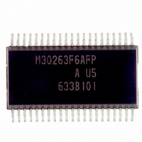
M30263F6AFP#U5A Renesas Electronics America, M30263F6AFP#U5A Datasheet - Page 183

M30263F6AFP#U5A
Manufacturer Part Number
M30263F6AFP#U5A
Description
IC M16C/26A MCU FLASH 42-SSOP
Manufacturer
Renesas Electronics America
Series
M16C™ M16C/Tiny/26r
Datasheet
1.M30260F3AGPU5A.pdf
(354 pages)
Specifications of M30263F6AFP#U5A
Core Processor
M16C/60
Core Size
16-Bit
Speed
20MHz
Connectivity
I²C, IEBus, SIO, UART/USART
Peripherals
DMA, PWM, Voltage Detect, WDT
Number Of I /o
33
Program Memory Size
48KB (48K x 8)
Program Memory Type
FLASH
Ram Size
2K x 8
Voltage - Supply (vcc/vdd)
2.7 V ~ 5.5 V
Data Converters
A/D 10x10b
Oscillator Type
Internal
Operating Temperature
-20°C ~ 85°C
Package / Case
42-SSOP
For Use With
R0K33026AS000BE - KIT DEV EVALUATION M16C/26A
Lead Free Status / RoHS Status
Lead free / RoHS Compliant
Eeprom Size
-
- Current page: 183 of 354
- Download datasheet (4Mb)
R
R
M
e
E
1
. v
J
6
Figure 13.1.3.1.1. Detection of Start and Stop Condition
0
C
2
9
0 .
B
2 /
0
0
6
13.1.3.1 Detection of Start and Stop Condition
13.1.3.2 Output of Start and Stop Condition
2
A
0
F
Whether a start or a stop condition has been detected is determined.
A start condition-detected interrupt request is generated when the SDA
to low while the SCL
when the SDA
Because the start and stop condition-detected interrupts share the interrupt control register and vec-
tor, check the BBS bit in the U2SMR register to determine which interrupt source is requesting the
interrupt.
A start condition is generated by setting the STAREQ bit in the U2SMR4 register to “1” (start).
A restart condition is generated by setting the RSTAREQ bit in the U2SMR4 register to “1” (start).
A stop condition is generated by setting the STPREQ bit in the U2SMR4 register to “1” (start).
The output procedure is described below.
(1) Set the STAREQ bit, RSTAREQ bit or STPREQ bit to “1” (start).
(2) Set the STSPSEL bit in the U2SMR4 register to “1” (output).
Make sure that no interrupts or DMA transfers will occur between (1) and (2).
The function of the STSPSEL bit is shown in Table 13.1.3.2.1 and Figure 13.1.3.2.1.
2
e
G
0 -
b
1 .
o r
2
NOTE:
3 to 6 cycles < setup time
3 to 6 cycles < hold time
0
, 5
u
0
p
1. When the PCLK1 bit in the PCLKR register is set to "1", the cycles indicates the f1SIO's
SDA2
SDA2
2
(
0
generation frequency cycles; when PCLK1 bit is set to "0", the cycles indicated the f2SIO's
generation frequency cycles.
M
0
7
1
(Start condition)
(Stop condition)
6
SCL2
C
page 164
2
2 /
pin changes state from low to high while the SCL
6
, A
2
M
pin is in the high state. A stop condition-detected interrupt request is generated
1
f o
6
C
3
(1)
2
2 /
(1)
9
6
, B
M
1
Setup time
6
C
2 /
6
) T
Hold time
2
pin is in the high state.
2
pin changes state from high
13. Serial I/O
Related parts for M30263F6AFP#U5A
Image
Part Number
Description
Manufacturer
Datasheet
Request
R

Part Number:
Description:
KIT STARTER FOR M16C/29
Manufacturer:
Renesas Electronics America
Datasheet:

Part Number:
Description:
KIT STARTER FOR R8C/2D
Manufacturer:
Renesas Electronics America
Datasheet:

Part Number:
Description:
R0K33062P STARTER KIT
Manufacturer:
Renesas Electronics America
Datasheet:

Part Number:
Description:
KIT STARTER FOR R8C/23 E8A
Manufacturer:
Renesas Electronics America
Datasheet:

Part Number:
Description:
KIT STARTER FOR R8C/25
Manufacturer:
Renesas Electronics America
Datasheet:

Part Number:
Description:
KIT STARTER H8S2456 SHARPE DSPLY
Manufacturer:
Renesas Electronics America
Datasheet:

Part Number:
Description:
KIT STARTER FOR R8C38C
Manufacturer:
Renesas Electronics America
Datasheet:

Part Number:
Description:
KIT STARTER FOR R8C35C
Manufacturer:
Renesas Electronics America
Datasheet:

Part Number:
Description:
KIT STARTER FOR R8CL3AC+LCD APPS
Manufacturer:
Renesas Electronics America
Datasheet:

Part Number:
Description:
KIT STARTER FOR RX610
Manufacturer:
Renesas Electronics America
Datasheet:

Part Number:
Description:
KIT STARTER FOR R32C/118
Manufacturer:
Renesas Electronics America
Datasheet:

Part Number:
Description:
KIT DEV RSK-R8C/26-29
Manufacturer:
Renesas Electronics America
Datasheet:

Part Number:
Description:
KIT STARTER FOR SH7124
Manufacturer:
Renesas Electronics America
Datasheet:

Part Number:
Description:
KIT STARTER FOR H8SX/1622
Manufacturer:
Renesas Electronics America
Datasheet:

Part Number:
Description:
KIT DEV FOR SH7203
Manufacturer:
Renesas Electronics America
Datasheet:


