MC908MR32CFUE Freescale Semiconductor, MC908MR32CFUE Datasheet - Page 97
MC908MR32CFUE
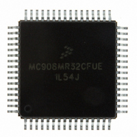
Manufacturer Part Number
MC908MR32CFUE
Description
IC MCU 8MHZ 32K FLASH 64-QFP
Manufacturer
Freescale Semiconductor
Series
HC08r
Datasheet
1.MC908MR16CFUE.pdf
(282 pages)
Specifications of MC908MR32CFUE
Core Processor
HC08
Core Size
8-Bit
Speed
8MHz
Connectivity
SCI, SPI
Peripherals
LVD, POR, PWM
Number Of I /o
44
Program Memory Size
32KB (32K x 8)
Program Memory Type
FLASH
Ram Size
768 x 8
Voltage - Supply (vcc/vdd)
4.5 V ~ 5.5 V
Data Converters
A/D 10x10b
Oscillator Type
Internal
Operating Temperature
-40°C ~ 85°C
Package / Case
64-QFP
Processor Series
HC08MR
Core
HC08
Data Bus Width
8 bit
Data Ram Size
768 B
Interface Type
SCI/SPI
Maximum Clock Frequency
8.2 MHz
Number Of Programmable I/os
44
Number Of Timers
6
Operating Supply Voltage
0 V to 5 V
Maximum Operating Temperature
+ 85 C
Mounting Style
SMD/SMT
Development Tools By Supplier
FSICEBASE, M68CBL05CE
Minimum Operating Temperature
- 40 C
On-chip Adc
10-ch x 10-bit
Lead Free Status / RoHS Status
Lead free / RoHS Compliant
Eeprom Size
-
Lead Free Status / Rohs Status
Lead free / RoHS Compliant
Available stocks
Company
Part Number
Manufacturer
Quantity
Price

Company:
Part Number:
MC908MR32CFUE
Manufacturer:
Freescale Semiconductor
Quantity:
10 000
Part Number:
MC908MR32CFUE
Manufacturer:
NXP/恩智浦
Quantity:
20 000


Chapter 9
Low-Voltage Inhibit (LVI)
9.1 Introduction
This section describes the low-voltage inhibit (LVI) module, which monitors the voltage on the V
and can force a reset when the V
9.2 Features
Features of the LVI module include:
9.3 Functional Description
Figure 9-1
contains a bandgap reference circuit and comparator. The LVI power bit, LVIPWR, enables the LVI to
monitor V
falls below a voltage, V
V
LVIRST are in the configuration register (CONFIG). See
Freescale Semiconductor
LVRX
•
•
•
•
Programmable LVI reset
Programmable power consumption
Digital filtering of V
Selectable LVI trip voltage
and V
DD
shows the structure of the LVI module. The LVI is enabled out of reset. The LVI module
FROM LVISCR
LVHX
voltage. The LVI reset bit, LVIRST, enables the LVI module to generate a reset when V
V
DETECTOR
TRPSEL
DD
LOW V
are determined by the TRPSEL bit in the LVISCR (see
DD
LVRX
V
V
DD
DD
DD
MC68HC908MR32 • MC68HC908MR16 Data Sheet, Rev. 6.1
> LVItrip = 0
< LVItrip = 1
, and remains at or below that level for nine or more consecutive CGMXCLK.
pin level
CPU CLOCK
Figure 9-1. LVI Module Block Diagram
ANLGTRIP
DD
FROM CONFIG
LVIPWR
voltage falls to the LVI trip voltage.
DIGITAL FILTER
V
DD
LVIOUT
Chapter 5 Configuration Register
FROM CONFIG
LVIRST
Figure
9-2). LVIPWR and
LVI RESET
(CONFIG).
DD
pin
DD
97
Related parts for MC908MR32CFUE
Image
Part Number
Description
Manufacturer
Datasheet
Request
R

Part Number:
Description:
Manufacturer:
Freescale Semiconductor, Inc
Datasheet:
Part Number:
Description:
Manufacturer:
Freescale Semiconductor, Inc
Datasheet:
Part Number:
Description:
Manufacturer:
Freescale Semiconductor, Inc
Datasheet:
Part Number:
Description:
Manufacturer:
Freescale Semiconductor, Inc
Datasheet:
Part Number:
Description:
Manufacturer:
Freescale Semiconductor, Inc
Datasheet:
Part Number:
Description:
Manufacturer:
Freescale Semiconductor, Inc
Datasheet:
Part Number:
Description:
Manufacturer:
Freescale Semiconductor, Inc
Datasheet:
Part Number:
Description:
Manufacturer:
Freescale Semiconductor, Inc
Datasheet:
Part Number:
Description:
Manufacturer:
Freescale Semiconductor, Inc
Datasheet:
Part Number:
Description:
Manufacturer:
Freescale Semiconductor, Inc
Datasheet:
Part Number:
Description:
Manufacturer:
Freescale Semiconductor, Inc
Datasheet:
Part Number:
Description:
Manufacturer:
Freescale Semiconductor, Inc
Datasheet:
Part Number:
Description:
Manufacturer:
Freescale Semiconductor, Inc
Datasheet:
Part Number:
Description:
Manufacturer:
Freescale Semiconductor, Inc
Datasheet:
Part Number:
Description:
Manufacturer:
Freescale Semiconductor, Inc
Datasheet: