MC908MR32CFUE Freescale Semiconductor, MC908MR32CFUE Datasheet - Page 62
MC908MR32CFUE
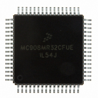
Manufacturer Part Number
MC908MR32CFUE
Description
IC MCU 8MHZ 32K FLASH 64-QFP
Manufacturer
Freescale Semiconductor
Series
HC08r
Datasheet
1.MC908MR16CFUE.pdf
(282 pages)
Specifications of MC908MR32CFUE
Core Processor
HC08
Core Size
8-Bit
Speed
8MHz
Connectivity
SCI, SPI
Peripherals
LVD, POR, PWM
Number Of I /o
44
Program Memory Size
32KB (32K x 8)
Program Memory Type
FLASH
Ram Size
768 x 8
Voltage - Supply (vcc/vdd)
4.5 V ~ 5.5 V
Data Converters
A/D 10x10b
Oscillator Type
Internal
Operating Temperature
-40°C ~ 85°C
Package / Case
64-QFP
Processor Series
HC08MR
Core
HC08
Data Bus Width
8 bit
Data Ram Size
768 B
Interface Type
SCI/SPI
Maximum Clock Frequency
8.2 MHz
Number Of Programmable I/os
44
Number Of Timers
6
Operating Supply Voltage
0 V to 5 V
Maximum Operating Temperature
+ 85 C
Mounting Style
SMD/SMT
Development Tools By Supplier
FSICEBASE, M68CBL05CE
Minimum Operating Temperature
- 40 C
On-chip Adc
10-ch x 10-bit
Lead Free Status / RoHS Status
Lead free / RoHS Compliant
Eeprom Size
-
Lead Free Status / Rohs Status
Lead free / RoHS Compliant
Available stocks
Company
Part Number
Manufacturer
Quantity
Price

Company:
Part Number:
MC908MR32CFUE
Manufacturer:
Freescale Semiconductor
Quantity:
10 000
Part Number:
MC908MR32CFUE
Manufacturer:
NXP/恩智浦
Quantity:
20 000


Clock Generator Module (CGM)
Exceeding the recommended maximum bus frequency or VCO frequency can crash the MCU.
4.3.2.5 Special Programming Exceptions
The programming method described in
exceptions. A value of 0 for N or L is meaningless when used in the equations given. To account for these
exceptions:
4.3.3 Base Clock Selector Circuit
This circuit is used to select either the crystal clock, CGMXCLK, or the VCO clock, CGMVCLK, as the
source of the base clock, CGMOUT. The two input clocks go through a transition control circuit that waits
up to three CGMXCLK cycles and three CGMVCLK cycles to change from one clock source to the other.
During this time, CGMOUT is held in stasis. The output of the transition control circuit is then divided by
62
5. Calculate the bus frequency, f
6. If the calculated f
7. Using the value 4.9152 MHz for f
8. Calculate the VCO center-of-range frequency, f
9. Program the PLL registers accordingly:
•
•
another f
multiplier controls the frequency range of the PLL.
between the minimum and maximum frequencies attainable by the PLL.
For proper operation,
A 0 value for N is interpreted exactly the same as a value of 1.
A 0 value for L disables the PLL and prevents its selection as the source for the base clock. See
4.3.3 Base Clock Selector
a. In the upper four bits of the PLL programming register (PPG), program the binary equivalent
b. In the lower four bits of the PLL programming register (PPG), program the binary equivalent
Example: L =
Example: f
of N.
of L.
RCLK
.
VRS
Example: N =
BUS
f
4.9152 MHz
VRS
MC68HC908MR32 • MC68HC908MR16 Data Sheet, Rev. 6.1
= 7 x 4.9152 MHz = 34.4 MHz
32 MHz
is not within the tolerance limits of the application, select another f
L = round
– f
VCLK
Circuit.
BUS
32 MHz
4 MHz
| ≤
NOM
= 7 MHz
(
4.3.2.4 Programming the PLL
, and compare f
f
f
f
NOM
VCLK
NOM
, calculate the VCO linear range multiplier, L. The linear range
2
f
VRS
f
BUS
CAUTION
= 8 MHz
)
= L x f
=
f
VRS
VCLK
4
NOM
BUS
. The center-or-range frequency is the midpoint
with f
BUSDES
does not account for possible
.
Freescale Semiconductor
BUSDES
or
Related parts for MC908MR32CFUE
Image
Part Number
Description
Manufacturer
Datasheet
Request
R

Part Number:
Description:
Manufacturer:
Freescale Semiconductor, Inc
Datasheet:
Part Number:
Description:
Manufacturer:
Freescale Semiconductor, Inc
Datasheet:
Part Number:
Description:
Manufacturer:
Freescale Semiconductor, Inc
Datasheet:
Part Number:
Description:
Manufacturer:
Freescale Semiconductor, Inc
Datasheet:
Part Number:
Description:
Manufacturer:
Freescale Semiconductor, Inc
Datasheet:
Part Number:
Description:
Manufacturer:
Freescale Semiconductor, Inc
Datasheet:
Part Number:
Description:
Manufacturer:
Freescale Semiconductor, Inc
Datasheet:
Part Number:
Description:
Manufacturer:
Freescale Semiconductor, Inc
Datasheet:
Part Number:
Description:
Manufacturer:
Freescale Semiconductor, Inc
Datasheet:
Part Number:
Description:
Manufacturer:
Freescale Semiconductor, Inc
Datasheet:
Part Number:
Description:
Manufacturer:
Freescale Semiconductor, Inc
Datasheet:
Part Number:
Description:
Manufacturer:
Freescale Semiconductor, Inc
Datasheet:
Part Number:
Description:
Manufacturer:
Freescale Semiconductor, Inc
Datasheet:
Part Number:
Description:
Manufacturer:
Freescale Semiconductor, Inc
Datasheet:
Part Number:
Description:
Manufacturer:
Freescale Semiconductor, Inc
Datasheet: